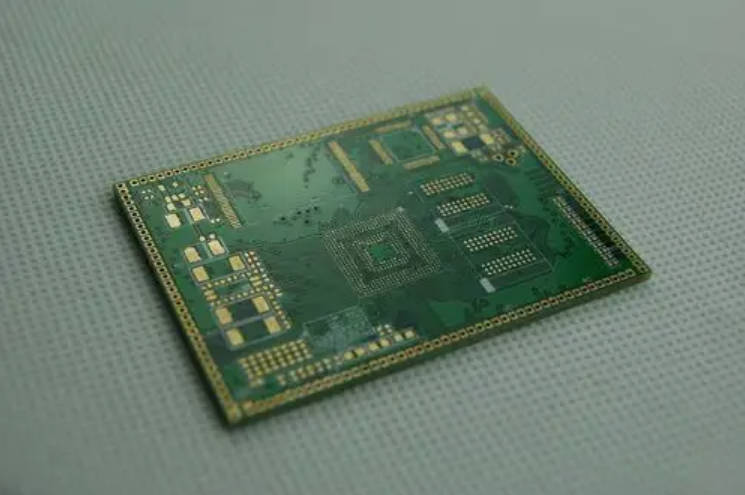
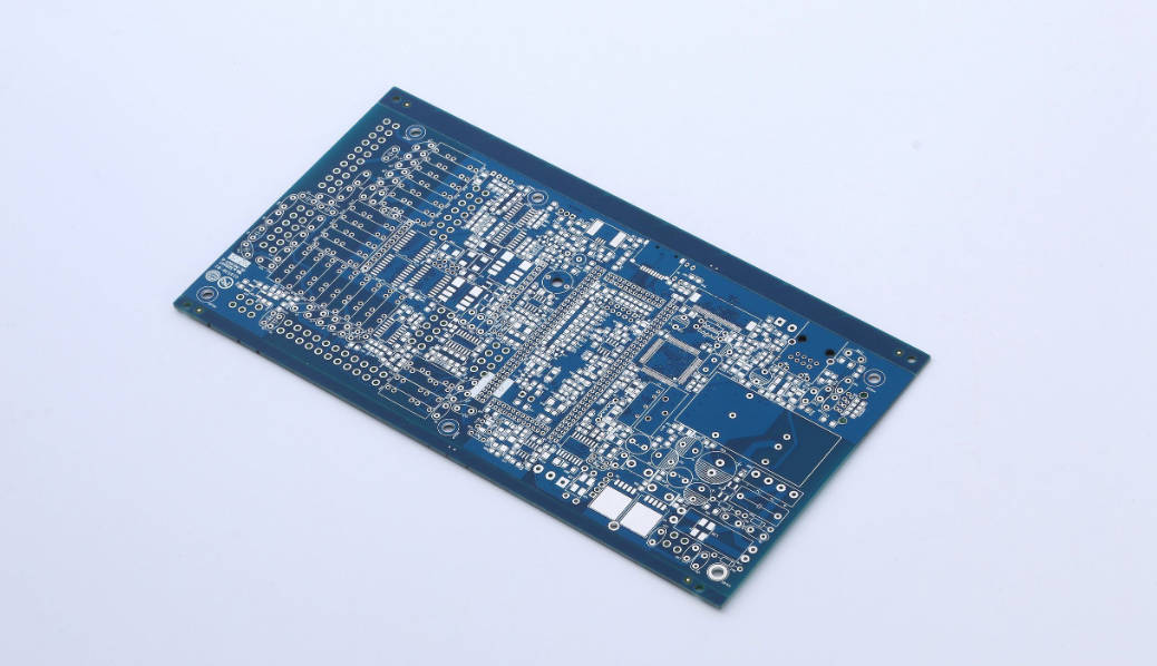
In the complex journey of electronic hardware development, there comes a pivotal moment when a standard 6-layer design no longer suffices. Perhaps your signal speeds have reached the gigahertz range, or your component density has become so high that routing feels like an impossible puzzle. If you find yourself at this crossroads, you are likely considering the transition to an 8-layer board.
Deciding between a 6 layer PCB vs 8 layer PCB is one of the most critical strategic choices an engineering team can make. It is a decision that balances raw technical performance against the cold reality of manufacturing budgets. In this guide, we will share a professional deep dive into these two multilayer architectures, helping you understand not just the “how,” but the “why” behind choosing the right stackup for your mission-critical projects.
1. Introduction: The Strategic Leap to High-Layer Counts
For many designers, the 6-layer PCB is the “sweet spot” for moderately complex industrial and consumer electronics. It offers a decent balance of signal routing and power distribution. However, as modern ICs (Integrated Circuits) become faster and more compact, the limitations of a 6-layer board—specifically regarding electromagnetic interference (EMI) and signal integrity—become apparent.
The transition from 6 to 8 layers is more than just adding two sheets of copper; it is a fundamental shift toward professional-grade signal integrity management. While the initial reaction to an 8-layer board is often concern over increased costs, the “peace of mind” gained from superior EMC compliance, stable power delivery, and reduced design “re-spins” often makes it the more economical choice in the long run.
2. Anatomy of the Stackup: Comparing the Architecture
To understand the performance gap, we must look at how these layers are physically organized. The arrangement of signal, ground, and power layers (the stackup) dictates how electromagnetic fields behave within the board.
The Standard 6-Layer Configuration
A typical 6-layer stackup is arranged as follows:
-
Top (Signal)
-
Internal Layer 1 (Ground Plane)
-
Internal Layer 2 (Signal/High-speed)
-
Internal Layer 3 (Signal/Power)
-
Internal Layer 4 (Power Plane)
-
Bottom (Signal)
While functional, this layout often forces designers to place signal layers adjacent to power planes rather than ground planes, which can compromise the return path for high-speed signals.
The 8-Layer Advantage: Interleaved Precision
An 8-layer board introduces a level of symmetry and “tight coupling” that is difficult to achieve with fewer layers. A professional 8-layer stackup might look like this:
-
Signal 1
-
Ground Plane 1
-
Signal 2 (High-speed)
-
Ground Plane 2
-
Power Plane
-
Signal 3 (High-speed)
-
Ground Plane 3
-
Signal 4
The primary structural advantage of an 8-layer PCB is the ability to sandwich every critical signal layer between two ground planes or a ground and a power plane, creating a shielded environment that minimizes noise and crosstalk.
3. The “7-Layer” Mystery: Why It Doesn’t Exist
One common question from users is: “If I only need a little more space than 6 layers provide, can I just design a 7-layer PCB?”
The short answer is no. In the world of PCB fabrication, odd-numbered layer counts are highly discouraged. Manufacturing a PCB with an odd number of layers, such as 7 layers, leads to structural asymmetry which causes the board to warp or “potato chip” during the high-temperature lamination and soldering processes.
Because PCBs are built using a core and prepreg layers, they must be balanced around the center. If you have three layers on one side and four on the other, the mechanical stress is uneven. Therefore, if your design requires more than 6 layers, your fabricator will almost certainly move you directly to an 8-layer stackup to ensure board flatness and manufacturing yield.
4. Performance Deep Dive: Signal Integrity & EMI
In high-speed digital design, the PCB is not just a carrier for components; it is a complex network of transmission lines.
Superior EMI Shielding
Electromagnetic Interference (EMI) is the biggest hurdle in getting a product to market. An 8-layer PCB offers a significant performance boost in EMI suppression, often providing up to 20dB more noise reduction than a 6-layer board by allowing for more dedicated ground planes that provide a low-impedance return path for every signal.
Managing Crosstalk and Impedance
When you have high-speed buses like DDR4, DDR5, or PCIe, crosstalk (signal bleeding between traces) can cause data corruption. In an 8-layer design, you can use the extra layers to:
-
Increase the distance between parallel signal traces.
-
Isolate sensitive analog signals from “noisy” digital signals using internal ground layers as shields.
-
Achieve much tighter control over characteristic impedance, which is vital for maintaining signal quality over long trace lengths.
5. Routing Density and High-Pin-Count BGAs
As components shrink, the “fan-out” (the process of routing pins away from a chip) becomes a nightmare. Fine-pitch Ball Grid Arrays (BGAs) with a pitch of 0.5mm or less often cannot be fully routed on a 6-layer board.
If your design utilizes high-pin-count BGA components, an 8-layer PCB is frequently the technical minimum required to provide enough internal routing channels for signal “escape” without resorting to extremely expensive micro-vias or blind/buried via technology. By utilizing layers 3, 4, 5, and 6 for internal routing, you keep the top and bottom layers clean for component placement and surface traces, reducing the overall footprint of the device.
6. Thermal Management: Keeping Cool Under Pressure
Heat dissipation is a critical factor for industrial controllers, power converters, and high-performance processors.
The additional copper mass in an 8-layer PCB acts as a much more efficient heat sink than a 6-layer board, allowing thermal energy to spread horizontally across internal planes and dissipate through the board’s surface more effectively.
In a 6-layer board, you might only have two planes (Power and Ground) to help with heat. In an 8-layer board, you might have four or more planes. This extra copper helps prevent “hot spots” that can degrade component performance or lead to premature hardware failure.
7. The Economic Reality: Cost vs. Long-Term Value
Let’s address the elephant in the room: the price tag.
Typically, the manufacturing cost of an 8-layer PCB is approximately 30% to 40% higher than a 6-layer PCB because it requires more raw materials (copper and prepreg), additional lamination cycles, and more intensive quality control inspections.
However, looking at the unit price of the bare board is a narrow perspective. You must consider the Total Cost of Development:
-
Reduced Re-spins: A 6-layer design pushed to its limit is more likely to fail EMI testing, requiring a costly redesign and a second round of prototyping.
-
Faster Time-to-Market: Easier routing means less time spent in the design phase.
-
Certification Success: Passing FCC or CE testing on the first try can save thousands of dollars in lab fees.
8. Comparison Table: 6-Layer vs. 8-Layer at a Glance
| Feature | 6-Layer PCB | 8-Layer PCB |
| Typical Stackup | 4 Signal, 2 Plane | 4 Signal, 4 Plane (or 5S/3P) |
| EMI Suppression | Good | Excellent |
| Impedance Control | Moderate | Very Precise |
| BGA Fan-out | Challenging for <0.8mm pitch | Ideal for <0.5mm pitch |
| Heat Dissipation | Standard | High Performance |
| Relative Cost | 1.0 (Baseline) | 1.3 – 1.4x |
| Manufacturing Complexity | Medium | High |
9. Decision Guide: When Should You Pull the Trigger?
How do you know when it is time to move from 6 to 8 layers? Here is a professional checklist:
Stay with 6 Layers if:
-
Your highest signal frequency is below 100-200 MHz.
-
Your design uses mostly leaded components or large-pitch SMDs.
-
You have ample board space and don’t need to shrink the product size.
-
Your budget is extremely tight, and the application is not “mission-critical.”
Upgrade to 8 Layers if:
-
High-Speed Data: You are working with DDR4/5 memory, Gigabit Ethernet, or USB 3.1.
-
EMI Sensitive: Your product must pass stringent Class B EMI testing.
-
Dense BGAs: You are using FPGA or ARM processors with high pin counts.
-
Mission Critical: The product is for medical, aerospace, or automotive use where reliability is the top priority.
10. Conclusion: Choosing for the Future
Choosing between a 6 layer PCB and an 8 layer PCB is a decision that defines the quality of your engineering. While the 6-layer board is a reliable workhorse for many applications, the 8-layer board is the gateway to high-performance, compact, and compliant electronic design.
We sincerely believe that if your project involves high-speed data or strict EMI requirements, the investment in those two extra layers will pay for itself in reliability and speed to market. Don’t wait for a failed EMI test to make the switch; design for success from the very first layer.