Blog
Chiplet and 2.5D/3D Packaging: Substrate and PCB Requirements
See how chiplet and 2.5D/3D packaging change substrate and PCB requirements, from silicon interposers and RDL layers to CTE matching and warpage control.

See how chiplet and 2.5D/3D packaging change substrate and PCB requirements, from silicon interposers and RDL layers to CTE matching and warpage control.
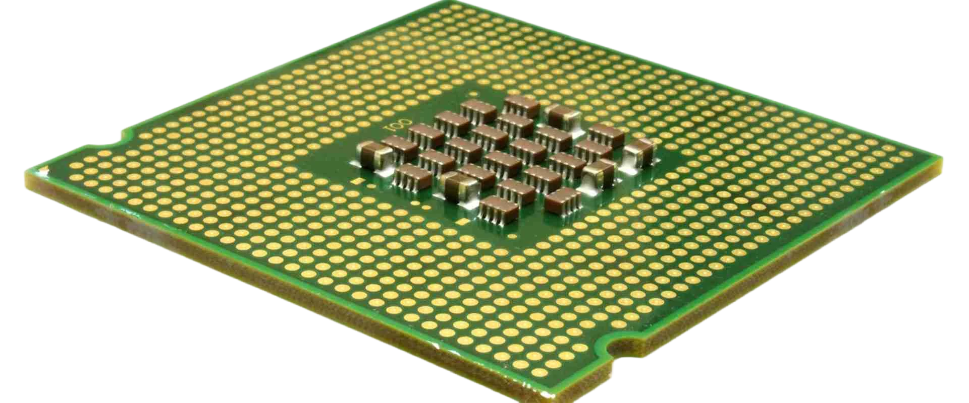
Compare IC substrate and standard PCB capability: feature size, via formation, material systems, flatness and volume economics, plus how to classify a design.
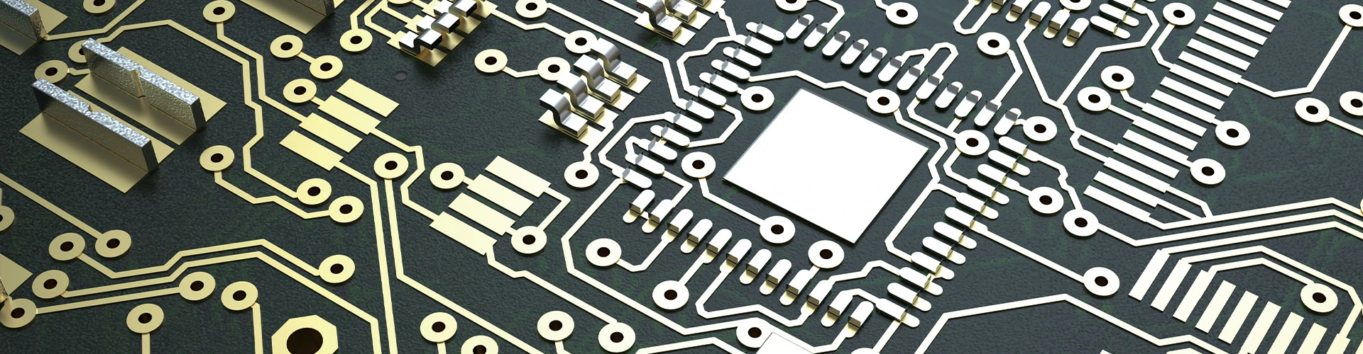
How chiplet and 2.5D/3D packaging shift interconnect onto interposers and substrates, and what that changes for board stack-up, power delivery and release.
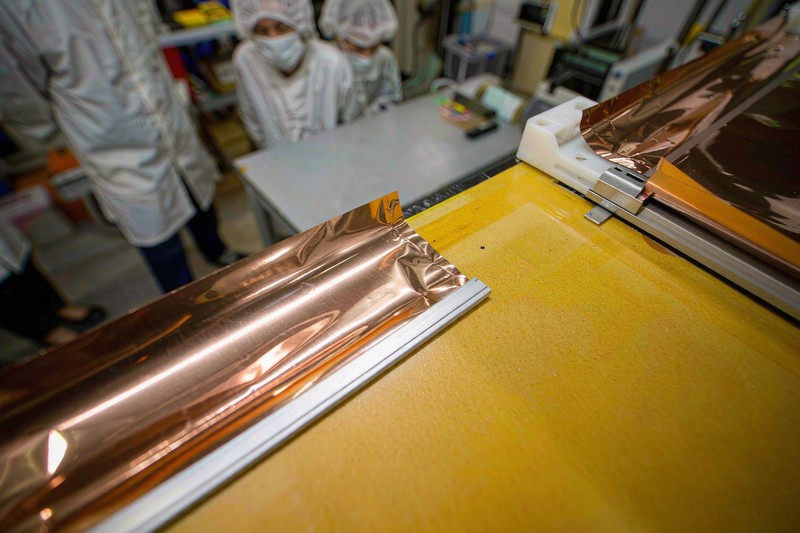
How ultra-thin copper foil down to 12µm improves etch geometry, where it is required for HDI and mSAP builds, and what it costs in handling and yield.
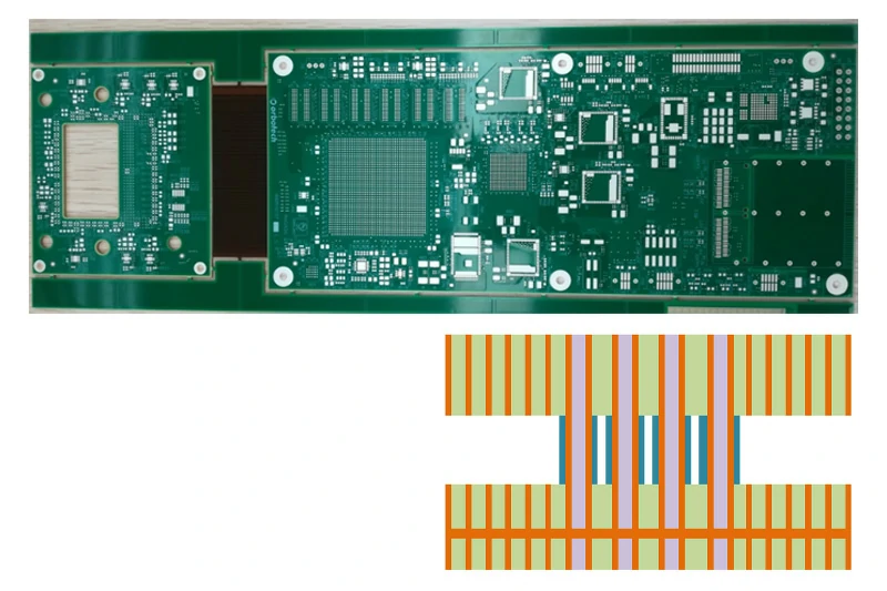
How AI server backplanes handle signal integrity, power delivery and press-fit connectors at 3-6 mm thickness, plus what to confirm before release.
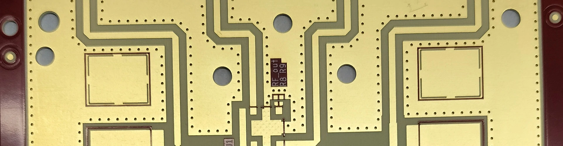
Compare M6, M7 and M8 low-loss CCL grades, what Df each tier delivers, where the crossover points sit, and how to choose the right laminate for your channel.
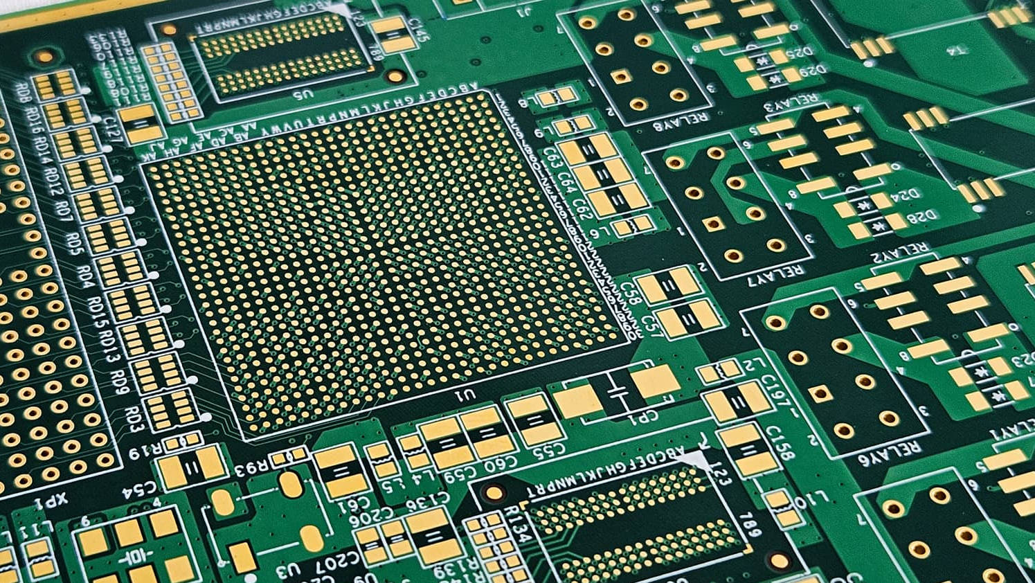
Compare mSAP and subtractive etching for fine-line PCBs. See why high-density and AI server designs are moving to semi-additive processing for trace and space below 50 micrometres.
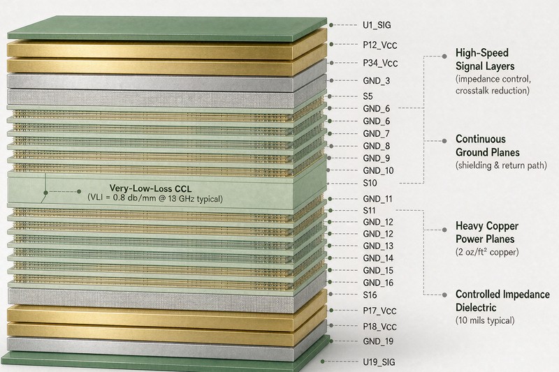
Practical guide to AI server PCB layer count, base material selection, and impedance control. Learn stackup principles, common mistakes, and RFQ specs.