When designing and manufacturing electronic circuits, the choice of printed circuit board (PCB) type is a critical decision, directly impacting a product’s performance, cost, and complexity. The fundamental comparison often boils down to double-sided PCBs and multilayer PCBs, each offering distinct advantages and disadvantages suited for different applications. While double-sided PCBs provide a cost-effective and straightforward solution for many common electronic devices, multilayer PCBs unlock significantly higher functionality, component density, and signal integrity crucial for advanced, high-performance electronics. Understanding their structural differences, fabrication processes, and impact on electrical characteristics is essential for engineers and designers to select the optimal board type for their specific project requirements.
Table of Contents
- Introduction to PCBs: The Foundation of Modern Electronics
- What is a Double-Sided PCB? Understanding Its Structure and Applications
- What is a Multilayer PCB? Exploring Its Complexity and Capabilities
- Multilayer PCB vs. Double-Sided PCB: A Detailed Comparison
- Making the Right Choice: When to Use Which PCB?
- Future Trends in PCB Technology
- Conclusion
- FAQs: Frequently Asked Questions
Introduction to PCBs: The Foundation of Modern Electronics
The Printed Circuit Board (PCB) is the unsung hero of virtually all modern electronic devices, serving as the physical foundation upon which electronic components are mounted and interconnected. From the simplest calculators to the most complex supercomputers, PCBs provide mechanical support and electrically connect components using conductive pathways, tracks, or signal traces etched from copper sheets laminated onto a non-conductive substrate. Without PCBs, the intricate wiring required for electronic circuits would be an unmanageable tangle, making compact, reliable, and mass-produced electronics impossible. The evolution of PCB technology, particularly the advancements from single-sided to double-sided and then to sophisticated multilayer designs, has been pivotal in driving miniaturization, enhancing performance, and reducing the cost of electronic products. This evolution allows designers to pack more functionality into smaller footprints while maintaining signal integrity and power distribution efficiency, directly addressing the ever-increasing demands for faster, smaller, and more powerful electronic devices across various industries.
What is a Double-Sided PCB? Understanding Its Structure and Applications
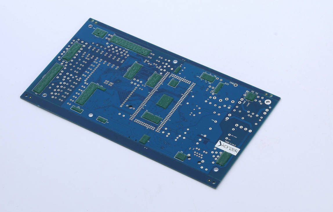
A double-sided PCB, also known as a two-layer PCB or dual-layer PCB, represents a significant step up from single-sided boards by allowing components and conductive traces to be routed on both the top and bottom surfaces of the board. This design greatly enhances the potential for circuit complexity and component density compared to its single-sided counterpart, which only utilizes one side. The ability to route traces on two layers means designers can create more intricate connections, effectively doubling the available routing area and allowing for crossover connections. This fundamental improvement has made double-sided PCBs a workhorse in the electronics industry, striking an excellent balance between complexity, manufacturability, and cost-effectiveness for a vast range of applications where modest component count and moderate circuit density are required.
Structural Anatomy of Double-Sided PCBs
The structure of a double-sided PCB is relatively straightforward yet highly effective. It consists of a central insulating substrate, typically made from fiberglass (FR-4 material being the most common), which provides mechanical strength and electrical isolation. Bonded to both the top and bottom surfaces of this substrate are thin layers of copper foil. These copper layers are selectively etched to form the conductive pathways, pads, and planes that constitute the electrical circuit. Crucially, vias (vertical interconnect access) are used to electrically connect traces on the top layer to traces on the bottom layer. These are typically plated through-holes (PTHs) that are drilled through the board and then plated with copper, creating a conductive path between the two sides. A solder mask layer is applied over the copper traces on both sides to protect them from oxidation, short circuits, and environmental factors, also defining the areas where components are to be soldered. Finally, a silkscreen layer is printed on top of the solder mask, providing human-readable labels for components, polarity indicators, and other useful markings for assembly and troubleshooting.
Fabrication Process for Double-Sided Boards
The fabrication of double-sided PCBs involves a series of precise steps. It begins with cutting the base material, the FR-4 laminate with copper on both sides, to the required size. Next, the circuit pattern is transferred onto the copper layers, usually through a photolithographic process. This involves applying a photoresist material, exposing it to UV light through a photomask (which defines the circuit layout), and then developing it to selectively remove the unexposed resist. The exposed copper is then etched away using chemical solutions, leaving behind the desired circuit traces and pads. After etching, the crucial step for double-sided boards is drilling. Holes for component leads (through-hole components) and vias are drilled through the entire board. These drilled holes are then chemically plated with copper, creating the conductive paths from one side to the other. Following plating, a solder mask is applied to both sides and cured, protecting the traces and defining the solderable areas. Finally, silkscreen printing adds component designators and other markings, and the board undergoes electrical testing, profiling (cutting into individual boards), and final inspection before packaging. This process is well-established and relatively straightforward, contributing to the lower cost of double-sided boards.
Key Characteristics, Advantages, and Limitations of Double-Sided PCBs
Double-sided PCBs offer a compelling set of characteristics that make them suitable for a broad range of electronic products. Their primary advantage lies in their cost-effectiveness, as the manufacturing process is less complex and utilizes standard materials and equipment, leading to lower production costs per board. They also boast a relatively short manufacturing lead time, facilitating quicker prototyping and faster time-to-market for products. From a design perspective, double-sided boards provide increased routing density compared to single-sided boards, allowing for more complex circuits and better utilization of board space without excessive component count. This makes them ideal for designs with a moderate number of components and interconnections. The reliability of double-sided boards is also generally high for their intended applications due to their simpler construction and fewer potential failure points compared to more complex multilayer designs. However, double-sided PCBs do come with inherent limitations. They are restricted in terms of component density and circuit complexity; dense designs with many interconnections can quickly exhaust the available routing space on just two layers. Signal integrity can be a challenge in high-speed applications due to longer trace lengths, lack of dedicated ground/power planes, and increased electromagnetic interference (EMI) susceptibility. Thermal management can also be less efficient compared to multilayer boards that can incorporate dedicated thermal planes. Ultimately, their simplicity is both their strength and their constraint.
Common Applications of Double-Sided PCBs
The versatility and cost-efficiency of double-sided PCBs make them suitable for a vast array of applications across various industries. They are frequently found in consumer electronics like **_LED lighting systems, calculators, remote controls, digital cameras, and basic audio equipment_**. In the telecommunications sector, they are used in **_simple communication modules, power supplies for networking equipment, and basic signal processing units_**. Industrial applications include **_motor control systems, power conversion devices, security systems, and industrial control panels_** where moderate complexity is sufficient. The automotive industry utilizes them for **_dashboard electronics, basic sensor modules, and lighting control systems_**. Moreover, they are popular in **_vending machines, basic medical devices, and even educational kits_** due to their robust nature and ease of assembly. Any product requiring a balance between functionality and cost, without demanding extremely high speeds, very dense component packing, or highly stringent EMI regulations, is a strong candidate for a double-sided PCB.
What is a Multilayer PCB? Exploring Its Complexity and Capabilities
A multilayer PCB takes the concept of a double-sided board and expands it vertically by stacking multiple layers of conductive material separated by insulating dielectric layers. This intricate construction allows for significantly higher component density, more complex circuit designs, and vastly improved electrical performance compared to simpler board types. By incorporating additional internal layers for signal routing, power distribution, and ground planes, multilayer PCBs address the critical challenges of miniaturization, high-speed data transmission, and electromagnetic compatibility (EMC) in modern electronics. They are the backbone of advanced technological products, enabling the sophisticated functionality and compact form factors that define today’s smart devices, high-performance computing, and complex communication systems, demonstrating a profound leap in PCB manufacturing and design capability.
Structural Anatomy of Multilayer PCBs
The structural anatomy of a multilayer PCB is a testament to sophisticated engineering. Unlike double-sided boards with just two copper layers, multilayer PCBs comprise three or more conductive copper layers, which can range from 4, 6, 8, to even over 100 layers in highly specialized applications. These copper layers are interleaved with alternating layers of insulating dielectric material, typically fiberglass (prepreg and core materials). The core layers are usually fully cured FR-4, while the prepreg layers are partially cured and act as an adhesive during lamination, bonding the layers together. The specific arrangement often includes dedicated planes for power (VCC) and ground (GND), which are crucial for stable voltage distribution and noise reduction. Signal traces are routed on other internal and external layers. Connectivity between these layers is achieved through various types of vias: through-hole vias (connecting all layers), blind vias (connecting an outer layer to one or more inner layers but not passing through the entire board), and buried vias (connecting two or more inner layers without reaching the outer layers). These advanced via technologies allow for extremely dense routing and improved signal integrity by minimizing stub lengths. The entire stack-up is then covered with a solder mask and silkscreen, similar to double-sided boards, but the internal complexity is exponentially greater.
Fabrication Process for Multilayer Boards
The fabrication process for multilayer PCBs is significantly more intricate and demanding than that for double-sided boards, involving several additional steps and higher precision. It begins by creating individual double-sided “cores” or single-sided “foils” with etched patterns for each layer. For inner layers, the copper foil laminated to a substrate (core) is etched with the circuit pattern. For outer layers, a similar process is followed, but these layers will become the outermost surfaces of the final board. Once all individual layers are prepared, they are meticulously aligned and stacked with alternating layers of prepreg (B-stage epoxy-impregnated glass fabric) and copper foil. This stack-up is then subjected to intense heat and pressure in a lamination press. The heat causes the prepreg to flow, melt, and then cure, permanently bonding all layers into a single, cohesive unit. After lamination, the panel is drilled for through-hole vias, blind vias, and buried vias. The process for buried vias might occur *before* lamination of certain cores, depending on the design. All drilled holes are then desmeared and chemically plated with copper to form conductive connections between the various layers. Subsequent steps include outer layer imaging and etching, application of solder mask, silkscreen printing, final electrical testing, and routing/profiling to separate individual boards. The precision required for layer alignment and the multiple lamination and drilling cycles contribute to the higher cost and longer lead times associated with multilayer PCB manufacturing.
Key Characteristics, Advantages, and Limitations of Multilayer PCBs
Multilayer PCBs are distinguished by their exceptional capabilities, making them indispensable for high-performance electronics. Their primary advantage is significantly **higher component density** and the ability to accommodate **more complex circuits** within a smaller form factor, leading to miniaturization of electronic products. The multiple layers provide abundant space for routing, allowing for optimized trace lengths and highly efficient power and ground planes. This greatly enhances **signal integrity** by reducing electromagnetic interference (EMI), crosstalk, and noise, which is critical for high-speed digital and analog circuits. Dedicated power and ground planes also improve **thermal management** by distributing heat more effectively. The increased structural rigidity from multiple bonded layers contributes to **enhanced durability and reliability** in demanding environments. Furthermore, multilayer boards offer unparalleled **design flexibility**, allowing engineers to integrate sophisticated features and intricate interconnects that would be impossible on simpler boards. However, these benefits come with substantial **limitations**. The manufacturing process is considerably **more complex and expensive**, involving precision lamination, multiple drilling steps, and specialized materials. This leads to **higher production costs** and **longer lead times** compared to double-sided boards. Troubleshooting and rework can also be more challenging due to the internal layers being inaccessible. The increased material layers also make the boards inherently thicker and heavier, though specific designs aim for thinner profiles where possible. Despite these drawbacks, for cutting-edge electronics, the advantages of multilayer PCBs far outweigh their complexities.
Common Applications of Multilayer PCBs
Due to their advanced capabilities, multilayer PCBs are prevalent in sophisticated electronic devices across a wide spectrum of industries. In **_consumer electronics_**, they are found in smartphones, tablets, smartwatches, high-end laptops, gaming consoles, and advanced digital cameras, where miniaturization and high processing power are paramount. The **_telecommunications_** industry heavily relies on them for network servers, routers, switches, base stations, and satellite communication systems, requiring high data rates and robust signal integrity. **_Medical devices_**, such as MRI machines, CT scanners, pacemakers, and advanced diagnostic equipment, utilize multilayer PCBs for their precision, reliability, and ability to handle complex data. The **_aerospace and defense_** sectors employ them in avionics, radar systems, guidance systems, and military-grade communication equipment, where extreme reliability and performance in harsh conditions are non-negotiable. Furthermore, **_automotive electronics_** for advanced driver-assistance systems (ADAS), engine control units (ECUs), infotainment systems, and autonomous driving modules frequently incorporate multilayer PCBs to manage vast amounts of sensor data and complex control algorithms. High-performance computing, industrial automation, and IoT devices with complex sensor arrays also widely adopt these boards, underscoring their role in powering the technological innovations of today and tomorrow.
Multilayer PCB vs. Double-Sided PCB: A Detailed Comparison
The choice between a multilayer PCB and a double-sided PCB is not merely about cost; it’s a strategic decision that impacts every aspect of an electronic product, from its electrical performance and physical dimensions to its manufacturing viability and market competitiveness. This comprehensive comparison delves into the critical differentiating factors, helping designers and engineers understand the trade-offs and select the most appropriate PCB technology for their specific application.
Performance and Signal Integrity
When it comes to **_performance and signal integrity_**, multilayer PCBs inherently offer significant advantages. With dedicated internal layers for ground and power planes, they provide superior impedance control, which is critical for high-frequency signals. These planes act as a shield, effectively reducing electromagnetic interference (EMI) and crosstalk between signal traces, leading to cleaner signals and less noise. Shorter signal paths, achieved by routing signals through inner layers and utilizing blind/buried vias, minimize inductance and capacitance, enabling faster clock speeds and higher data rates. This makes multilayer boards indispensable for high-speed digital circuits, RF applications, and sensitive analog circuits. In contrast, double-sided PCBs, lacking dedicated ground/power planes, struggle with impedance control, often suffer from higher noise levels, and are more susceptible to EMI. While adequate for lower-frequency signals and less demanding applications, achieving good signal integrity on a double-sided board for high-speed designs can be challenging and may require more complex routing techniques and careful component placement, often at the expense of board space.
Component Density and Board Size
The ability to achieve **_high component density and minimize board size_** is a major differentiator. Multilayer PCBs excel in this area due to their ability to route signals and distribute power across multiple internal layers. This vastly increases the available routing channels, allowing designers to pack more components onto a smaller surface area, especially with fine-pitch components and complex integrated circuits. The use of blind and buried vias further conserves surface space by connecting only the necessary layers, freeing up external layers for component placement. This miniaturization is crucial for compact consumer electronics like smartphones and wearables. Double-sided PCBs, by comparison, are limited to routing on just two outer layers. While efficient for moderate component counts, they quickly run out of routing space as complexity increases, often necessitating larger board dimensions to accommodate all components and their interconnections. This limitation directly impacts the form factor of the end product, making double-sided boards less suitable for applications where size and weight are critical constraints.
Manufacturing Complexity and Cost
The disparity in **_manufacturing complexity and cost_** is perhaps the most obvious distinction. Double-sided PCBs benefit from a relatively simpler and more streamlined fabrication process. With fewer layers, fewer alignment steps, and less specialized equipment, their production costs are significantly lower per unit, and their lead times are shorter. This makes them highly attractive for mass-produced, cost-sensitive products. Conversely, multilayer PCBs involve a far more intricate and demanding manufacturing sequence. The precise alignment and lamination of multiple layers, the specialized drilling for blind and buried vias, and the increased inspection requirements all contribute to a higher manufacturing complexity. This translates directly into substantially higher production costs and longer lead times. Specialized materials, higher quality control, and more advanced processing equipment further add to the expense. For this reason, selecting a multilayer board must be justified by the performance and density requirements that cannot be met by a simpler two-layer design.
Thermal Management
**_Thermal management_** is another critical aspect where multilayer PCBs often hold an advantage. With multiple conductive copper layers, particularly dedicated ground and power planes, multilayer boards can dissipate heat more effectively across a larger area. These large copper planes act as efficient heat sinks, drawing heat away from hot components and distributing it throughout the board, thus helping to maintain optimal operating temperatures for sensitive components. This is particularly important for high-power devices or densely packed circuits that generate significant heat. While thermal vias can be incorporated into double-sided PCBs to help transfer heat, the overall thermal dissipation capability is generally less efficient due to the absence of extensive internal copper planes. For applications where overheating is a concern, such as high-performance processors or power electronics, the superior thermal characteristics of multilayer PCBs can significantly improve reliability and extend component lifespan.
Design Flexibility and Routing Options
When it comes to **_design flexibility and routing options_**, multilayer PCBs offer an unparalleled degree of freedom. The availability of numerous internal layers provides a vast canvas for routing complex signal paths, implementing differential pairs, and creating optimal impedance-controlled transmission lines without constraints on the outer layers. Designers can strategically assign layers for specific signal types, power, and ground, leading to more organized and efficient layouts. The use of advanced via technologies like blind and buried vias further enhances routing efficiency by connecting only the necessary layers, minimizing space usage and signal stubs. This flexibility is crucial for integrating high-pin-count components like FPGAs and BGAs. Double-sided PCBs, on the other hand, are inherently more restrictive. With only two layers, routing becomes a “jigsaw puzzle” where designers must carefully manage trace crossings, often relying on generous spacing or employing numerous through-hole vias, which can consume valuable board space and potentially compromise signal integrity. This limitation often forces compromises in component placement or results in larger board dimensions, highlighting the superior adaptability of multilayer designs for intricate circuits.
Reliability and Durability
In terms of **_reliability and durability_**, both PCB types have their merits, though multilayer PCBs often offer enhanced robustness for complex systems. The multiple layers in a multilayer board, bonded together under high pressure and temperature, contribute to a greater overall structural rigidity. This makes them more resistant to warping, vibration, and mechanical stress, which is vital in applications exposed to harsh environments, such as aerospace or automotive electronics. The internal layers are also protected from external factors like humidity and dust, potentially leading to longer lifespans for the internal circuitry. While double-sided PCBs are also robust and reliable for many applications, their simpler construction means they might be more susceptible to flexing or warping under significant mechanical stress compared to the stiffer multilayer constructions. However, simpler designs also mean fewer potential manufacturing defects related to layer registration or complex via structures, which can sometimes impact multilayer board reliability. Ultimately, reliability often comes down to the quality of manufacturing and adherence to design guidelines for both types.
Time to Market
**_Time to market_** is a crucial business consideration, and here, double-sided PCBs typically have an advantage. Their simpler manufacturing process translates to faster fabrication times, allowing for quicker prototyping and more rapid production cycles. This agility can be a significant benefit for products with short development cycles or those that need to respond quickly to market demands. The ability to iterate designs quickly with lower NRE (Non-Recurring Engineering) costs associated with tooling also supports faster market entry. Multilayer PCBs, conversely, are characterized by longer manufacturing lead times due due to their complex production sequence involving multiple lamination, drilling, and plating steps. The intricate alignment required for internal layers and the specialized processes for blind/buried vias extend the fabrication timeline. While necessary for high-performance products, these longer lead times must be factored into project planning, potentially impacting the overall time to market and product launch schedules. For projects where rapid prototyping and quick turnaround are paramount, double-sided boards often present a more favorable option.
| Feature | Double-Sided PCB | Multilayer PCB |
|---|---|---|
| Layers | 2 (Top & Bottom) | 3 or more (typically 4, 6, 8, or higher) |
| Component Density | Moderate | High to very high |
| Circuit Complexity | Moderate | High to very high |
| Signal Integrity | Good for low-to-medium speeds; challenges with high speed | Excellent, superior impedance control, reduced EMI/crosstalk |
| Cost | Lower | Higher (due to complex manufacturing) |
| Manufacturing Complexity | Lower, simpler process | Higher, intricate lamination, drilling, alignment |
| Lead Time | Shorter | Longer |
| Board Size | Larger for complex circuits | Smaller, allows for miniaturization |
| Thermal Management | Adequate for moderate heat dissipation | Superior, dedicated planes act as heat sinks |
| Design Flexibility | Limited routing options | High, extensive routing paths, blind/buried vias |
| Applications | Consumer electronics (basic), LED lighting, power supplies, industrial controls | Smartphones, laptops, servers, medical devices, aerospace, high-speed networking |
Making the Right Choice: When to Use Which PCB?
The decision between a double-sided and a multilayer PCB is a crucial engineering trade-off that directly impacts product performance, manufacturability, cost, and time-to-market. There’s no universally “better” option; instead, the optimal choice hinges entirely on the specific requirements and constraints of the project. A thorough evaluation of factors such as circuit complexity, required performance (especially signal speed), physical size limitations, budget, and production volume is essential to ensure that the chosen PCB technology aligns perfectly with the product’s overall goals and strategic objectives. Misjudging this decision can lead to either an over-engineered, costly product or an under-performing device that fails to meet expectations.
Factors Influencing Your PCB Selection
Several key factors must be carefully weighed when making your PCB selection:
- Circuit Complexity and Component Density: How many components are there, and how tightly must they be packed? High pin-count ICs (e.g., BGAs, FPGAs) with many interconnections almost always demand multilayer boards.
- Electrical Performance Requirements (Speed, Signal Integrity, EMI): Are you dealing with high-frequency signals (e.g., GHz range)? Is precise impedance control necessary? Is electromagnetic interference (EMI) a critical concern? If so, the controlled impedance and dedicated planes of multilayer PCBs are often indispensable.
- Physical Size and Form Factor: Is miniaturization a primary goal? If the product needs to be very small or thin (e.g., wearables, smartphones), a multilayer PCB is usually the only viable option to achieve the necessary component density.
- Cost Constraints and Budget: How sensitive is the project to cost? Double-sided PCBs are significantly cheaper to manufacture, making them ideal for budget-constrained projects or high-volume, low-margin products.
- Time-to-Market and Production Volume: How quickly does the product need to be released? Double-sided boards offer faster prototyping and production. For high-volume manufacturing where every penny counts, the cost efficiency of double-sided boards can be a decisive factor if performance requirements allow.
- Power Distribution and Thermal Management: Are there high-power components that generate significant heat? Multilayer boards with dedicated power/ground planes offer superior thermal dissipation.
- Reliability and Durability: Will the device operate in harsh environments (vibration, temperature extremes)? The added rigidity of multilayer boards can be an advantage.
- Design and Manufacturing Expertise: Does your team and your chosen manufacturer have the expertise for complex multilayer designs and fabrication?
By systematically addressing these questions, engineers can logically determine whether the simpler, more economical double-sided PCB suffices or if the advanced capabilities and higher cost of a multilayer PCB are justified.
Scenarios Favoring Double-Sided PCBs
Double-sided PCBs are the preferred choice in numerous situations where their cost-effectiveness and simpler manufacturing outweigh the need for extreme complexity or high-speed performance. These boards are ideal for designs with a moderate number of components, where circuit complexity can be managed with two routing layers without excessive crossovers. Projects with tight budget constraints, where the bill of materials and manufacturing costs are paramount, will benefit from the lower production expenses of double-sided boards. Similarly, for applications that do not involve high-frequency signals or require stringent impedance control, double-sided PCBs offer adequate electrical performance. They are excellent for **_rapid prototyping and educational projects_**, allowing for quick iterations and faster design validation due to shorter lead times. Common real-world examples include simple power supplies, LED lighting modules, basic consumer electronics like remote controls, home appliances, automotive dashboard displays, and many industrial control systems that operate at lower frequencies. In essence, if the design can be successfully implemented with two layers while meeting all performance and size objectives, choosing a double-sided PCB will almost always result in a more economical and faster path to production.
Scenarios Favoring Multilayer PCBs
Multilayer PCBs become indispensable when the design demands high performance, compact size, and intricate functionality that cannot be achieved with two layers. They are the go-to solution for **_high-speed digital circuits_**, such as microprocessors, FPGAs, and high-speed memory interfaces, where signal integrity, controlled impedance, and minimal noise are critical. When **_miniaturization_** is a primary design goal – for instance, in smartphones, wearables, or medical implants – multilayer boards allow for dense component packing and complex routing within a small form factor. Projects involving **_high-pin-count components_** (e.g., BGAs with hundreds of pins) necessitate multilayer boards to accommodate the vast number of required interconnections. Furthermore, applications with **_strict electromagnetic compatibility (EMC) requirements_** benefit immensely from the dedicated ground and power planes of multilayer designs, which provide effective shielding and reduce EMI. Devices requiring **_efficient thermal management_** for high-power components also favor multilayer boards, as their extensive copper layers aid in heat dissipation. Ultimately, any advanced electronic system – from complex servers and networking equipment to sophisticated avionics and medical imaging devices – that pushes the boundaries of performance, density, and reliability will almost certainly leverage multilayer PCB technology.
Future Trends in PCB Technology
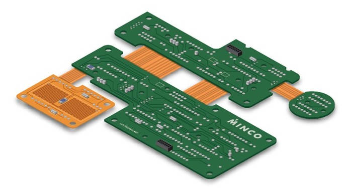
The evolution of electronics continues at an unprecedented pace, and PCB technology is evolving in tandem to meet ever-increasing demands. Future trends in PCB technology point towards even greater miniaturization, higher integration, and enhanced performance. We can expect to see wider adoption of **_High-Density Interconnect (HDI) PCBs_**, which utilize microvias, buried vias, and blind vias to achieve even finer line widths and spaces, enabling more compact and complex designs. The pursuit of faster data rates will drive advancements in **_materials science_**, with a focus on low-loss dielectric materials for high-frequency applications and improved thermal conductivity. **_Embedded component technology_**, where passive or even active components are integrated directly within the PCB layers, will become more prevalent, further reducing board size and improving performance by shortening signal paths. **_Flexible and rigid-flex PCBs_** will continue to gain traction, offering solutions for devices with irregular form factors or those requiring dynamic movement. Additionally, advancements in **_manufacturing processes_** such as additive manufacturing (3D printing of PCBs) and improved automation will enable more cost-effective production of highly complex boards, reduce waste, and allow for rapid prototyping of specialized designs. These innovations ensure that PCBs remain at the forefront of electronic development, adapting to the needs of emerging technologies like AI, IoT, 5G, and quantum computing.
Conclusion
In conclusion, the decision between a double-sided PCB and a multilayer PCB is not a matter of one being inherently “better” than the other, but rather a strategic engineering choice dictated by the specific requirements of an electronic design. Double-sided PCBs offer a cost-effective, straightforward, and reliable solution for a vast array of applications that demand moderate circuit complexity, reasonable component density, and do not involve stringent high-speed signal integrity challenges. They are ideal for projects where budget and time-to-market are critical. Conversely, multilayer PCBs are the powerhouse behind modern, high-performance electronics. They unlock unparalleled component density, superior signal integrity, efficient thermal management, and immense design flexibility, making them essential for complex, high-speed, and miniaturized devices found in cutting-edge industries. Ultimately, a thorough understanding of the distinct advantages, limitations, and manufacturing implications of each PCB type is paramount. By carefully assessing factors such as circuit complexity, performance demands, physical constraints, and cost, designers can make an informed decision that optimizes their product for functionality, manufacturability, and market success. The evolution of both technologies will continue, pushing the boundaries of what’s possible in electronic design.
FAQs: Frequently Asked Questions
What is the main difference between a multilayer PCB and a double-sided PCB?
The main difference lies in the number of conductive layers. A double-sided PCB has copper traces on its top and bottom surfaces (2 layers), while a multilayer PCB incorporates three or more conductive copper layers, which are separated by insulating dielectric materials and bonded together. This allows for significantly more complex circuit routing and component density in multilayer boards.
When should I choose a double-sided PCB?
You should choose a double-sided PCB when your design has moderate complexity, a relatively low component count, does not require ultra-high-speed signals, and when cost-effectiveness and faster manufacturing lead times are primary concerns. They are suitable for many consumer electronics, LED applications, simple power supplies, and industrial controls.
When is a multilayer PCB necessary?
A multilayer PCB is necessary for designs requiring high component density, miniaturization, complex high-speed digital or RF circuits, precise impedance control, superior signal integrity, and effective thermal management. Applications include smartphones, computers, servers, advanced medical devices, and aerospace electronics.
Are multilayer PCBs more expensive than double-sided PCBs?
Yes, multilayer PCBs are generally significantly more expensive than double-sided PCBs. This is due to their more complex manufacturing process, which involves multiple lamination cycles, precise layer alignment, and specialized drilling for blind and buried vias. The increased material cost and longer production times also contribute to the higher price.
Does the number of layers affect signal integrity?
Absolutely. Multilayer PCBs offer superior signal integrity. With dedicated ground and power planes, they provide better impedance control, reduce electromagnetic interference (EMI) and crosstalk, and allow for shorter, more optimized signal paths. Double-sided PCBs, lacking these dedicated planes, can struggle with signal integrity, especially at higher frequencies.
What are blind and buried vias?
Blind vias connect an outer layer of a multilayer PCB to one or more inner layers without passing through the entire board. Buried vias connect two or more inner layers without reaching the outer surfaces. Both types of vias are used in multilayer PCBs to maximize routing density and improve signal integrity by minimizing stub lengths, which helps reduce reflections in high-speed signals.
Can double-sided PCBs be used for high-frequency applications?
While possible for some lower-frequency RF applications with very careful design and layout techniques, double-sided PCBs are generally not ideal for high-frequency or high-speed digital applications. They lack the dedicated ground planes and controlled impedance structures that multilayer PCBs offer, making them more susceptible to signal integrity issues like crosstalk and EMI at higher frequencies.
How do PCB layers affect thermal management?
Multilayer PCBs generally offer better thermal management. The large copper planes (power and ground) within multilayer boards act as efficient heat sinks, distributing heat away from hot components across a larger area. While thermal vias can help on double-sided boards, the overall thermal dissipation capability is usually higher in multilayer designs due to the extensive internal copper mass.