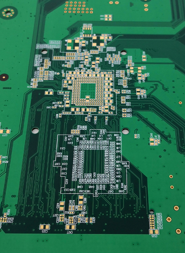
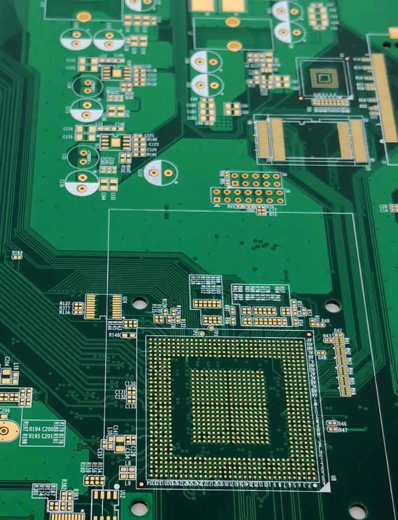
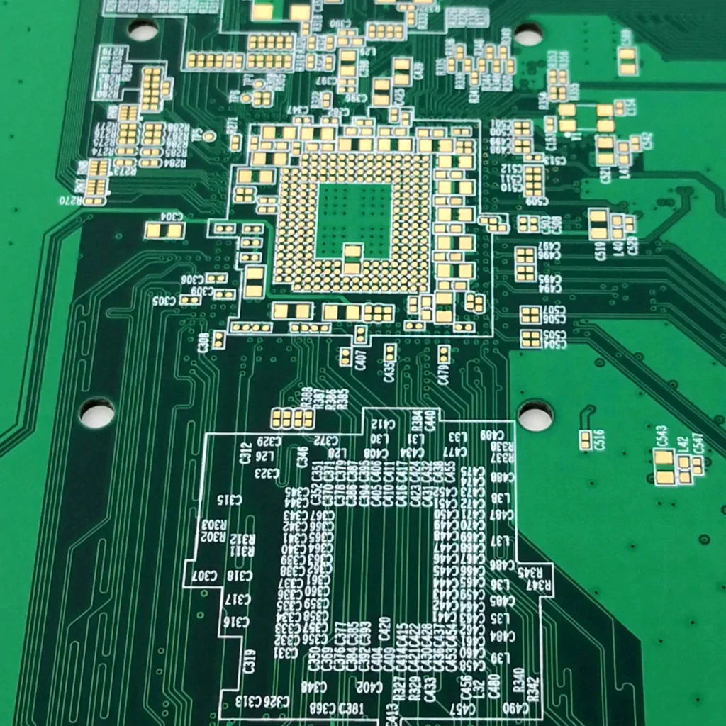
Impedance Control
At Mars PCB, we prioritize impeccable impedance control to ensure the highest quality for your electronic products.

What’s Impedance Control?
Impedance control is essential in PCB design, especially for high-speed digital applications such as RF communications, telecommunications, computing (>100MHz), and analog video (e.g., DDR, HDMI, Gigabit Ethernet). Variations in etching, layer thickness, and trace width can distort signals. To prevent this, our designers use precise layout techniques and parameter control to maintain consistent impedance along signal traces, which is crucial for avoiding reflections and signal distortion.
High-frequency signals require exact impedance control as PCB traces function as transmission lines. Any changes in impedance can cause signal reflections, degrading the signal and leading to timing errors. At Mars PCB, we consider trace width, spacing, the dielectric constant of PCB materials, and layer stack-up to match the transmission line impedance with signal requirements.
Telecommunications, computing (>100MHz), and analog video (e.g., DDR, HDMI, Gigabit Ethernet). Variations in etching, layer thickness, and trace width can distort signals. To prevent this, our designers use precise layout techniques and parameter control to maintain consistent impedance along signal traces, which is crucial for avoiding reflections and signal distortion.
Our dedication to delivering PCBs with precise impedance control goes beyond theoretical approaches. We utilize advanced design tools and simulations to determine optimal trace geometries and material properties. Mars PCB employs techniques such as controlled trace width, spacing, and stripline/microstrip configurations, along with impedance matching components like series resistors, to ensure controlled impedance. This precision is vital for maintaining signal integrity, which is critical in high-speed and high-frequency applications for reliable circuit performance.
In PCB design, impedance control is not merely a technical necessity—it’s a fundamental aspect of delivering top-quality electronic products. Choose Mars PCB as your partner, and we will help you achieve the level of impedance control required for the success of your electronic devices. Your satisfaction is our priority, and we are committed to ensuring it.

Factors that Influence Impedance
In PCB design, several factors influence impedance control and performance. Below, we explore these factors in detail, including trace width, thickness, dielectric properties, copper foil thickness, and solder mask thickness, to help you understand and manage the key elements of impedance.

Trace Width
The width of PCB traces is crucial for impedance control. Thinner traces result in higher impedance, while wider traces lead to lower impedance. Maintaining trace width within a tight tolerance, typically around ±10%, is essential for precise impedance control. Any gaps or interruptions in signal traces can disrupt the entire waveform, causing uneven impedance. Accurate control of trace width is achieved through meticulous etching processes, which involve engineering compensation to account for factors like etch undercut, lithographic errors, and pattern transfer errors.

Soldermask Thickness
Soldermask thickness also influences impedance, with a thinner solder mask generally resulting in higher impedance within a certain range. For instance, a single pass of solder mask printing can reduce single-ended impedance by 2 ohms and differential impedance by 8 ohms. The reduction effect doubles when printing two passes compared to one pass. However, after three or more passes, the impedance value stabilizes. Careful management of solder mask thickness is crucial for achieving precise impedance control.

Copper Thickness
The thickness of the copper foil used for PCB traces inversely affects impedance. Thicker copper foils lead to lower impedance. Copper thickness can be controlled through techniques such as pattern electroplating or by selecting base material copper foils with the appropriate thickness to meet impedance requirements.

Dielectric Constant
The dielectric constant of the PCB material significantly impacts impedance. A higher dielectric constant results in lower impedance. Material selection is the primary method of controlling the dielectric constant. Different PCB materials have distinct dielectric constants, often related to the resin materials used. For example, FR4 materials have dielectric constants ranging from 3.9 to 4.5, which decrease with increasing frequency. PTFE materials, on the other hand, feature dielectric constants between 2.2 and 3.9. High-speed signal transmission often requires higher impedance values, necessitating materials with lower dielectric constants.

Dielectric Thickness
The thickness of the dielectric material between signal layers directly affects impedance. Thicker dielectric layers correspond to higher impedance. Achieving consistent dielectric thickness is a complex process influenced by various factors, including the resin content in semicured sheets and the precision of the pressing plate during lamination. Engineering design, press plate control, and tolerance management are critical for obtaining the desired dielectric layer thickness.
Impedance Considerations for Other Features
In optimizing PCB design, considering impedance for other features is also essential. Here are several aspects related to impedance management, encompassing not only impedance for PCB traces but also for other components:

Vias:
Impedance of vias depends on their diameter, anti-pad size, and clearances with copper planes.
Signal via impedance is typically tuned to be between 50-75Ω.
Minimize stubs by positioning vias at layer junctions.
Creating fence shapes around via anti-pads on the reference plane achieves controlled impedance.
Planes:
Impedance of power and ground planes is critical for decoupling.
Solid fills with multiple vias lower impedance.
Avoiding cuts and splits helps maintain consistent plane impedance.
Pads:
Matched Launch – Pads should be sized and shaped to match trace width to ensure impedance matching.
Solder Mask Over Pad (SMOBC) – Allows for smaller pads while maintaining the desired clearance.
In summary, in PCB design, simulation can provide estimates of impedance, but measured impedances on actual PCB configurations take precedence over simulations. Therefore, actual measurements must be conducted to validate and optimize impedance. Impedance management is crucial for ensuring signal integrity and circuit performance, so all the aspects mentioned above need to be considered holistically.
Common Controlled Impedance Types
Here’s a detailed explanation of the different types of impedance.In summary, these various types of impedance, including characteristic impedance, differential impedance, odd-mode impedance, even-mode impedance, and common-mode impedance, play essential roles in PCB design, especially in high-speed data transmission. Understanding and controlling these impedance values are critical for ensuring signal quality and minimizing signal integrity issues in electronic circuits.
In electronic products like computers and wireless communication devices, the energy transmitted through PCB traces often consists of square wave signals, also known as pulse signals. The resistance encountered by these signals is referred to as characteristic impedance. It represents the impedance value that a transmission line appears to have when it is infinitely long.
Differential impedance is associated with a pair of traces where two identical signals with opposite polarities are driven. These signals are transmitted through two separate traces and, at the receiving end, the two differential signals are subtracted from each other. The impedance between these two lines is known as differential impedance (Z_diff). Maintaining a consistent differential impedance is critical for ensuring signal integrity in high-speed data transmission.
Odd-mode impedance (Z_odd) refers to the impedance of a single line with respect to ground. In a differential pair, the impedance values of the two lines are the same, and this impedance value is known as odd-mode impedance. It is used to describe the impedance characteristics when the signals are in anti-phase (180 degrees out of phase).
Even-mode impedance (Z_even) is associated with a pair of traces where two identical signals with the same polarity are driven. When these two lines are connected together, the impedance between them is referred to as even-mode impedance. This impedance is important for understanding how signals behave when they are in phase.
Common-mode impedance (Z_common) is the impedance of a single line with respect to ground, similar to odd-mode impedance. However, common-mode impedance is typically larger than odd-mode impedance. It describes the impedance characteristics when both lines in a differential pair are subjected to the same external interference or noise.
In summary, these various types of impedance, including characteristic impedance, differential impedance, odd-mode impedance, even-mode impedance, and common-mode impedance, play essential roles in PCB design, especially in high-speed data transmission. Understanding and controlling these impedance values are critical for ensuring signal quality and minimizing signal integrity issues in electronic circuits.
How to Measure Impedance?
Accurate impedance measurement on a PCB is critical to ensure signal integrity in high-frequency applications.
There are two common methods for measuring impedance: Time Domain Reflectometry (TDR) and Vector Network Analyzer (VNA).
Here’s a detailed explanation of each method:


TDR Method
TDR is a widely used technique for PCB impedance measurement, especially for single-ended and differential transmission lines. It relies on measuring reflections in the time domain and analyzing them to determine the impedance. Here’s a step-by-step breakdown:
Select the Test Line:Choose a specific section of the PCB’s transmission line that you want to measure for impedance. This section should represent the PCB’s impedance characteristics.
Connect TDR Probe:Connect the TDR instrument’s probe to the starting point of the chosen test line. Ensure a secure and low-impedance connection to avoid measurement inaccuracies.
Send Pulse Signals:Use the TDR instrument to send a short pulse signal down the test line. The pulse travels along the line and encounters impedance variations, causing reflections.
Record Reflections:The TDR instrument records the reflections of the pulse as it encounters impedance changes along the transmission line. These reflections are displayed as a waveform on the instrument’s screen.
Analyze Reflections:Analyze the reflected waveform to determine the impedance characteristics of the transmission line. Impedance changes, such as mismatches or discontinuities, will be visible in the waveform.
Calculate Impedance:By interpreting the waveform, you can calculate the characteristic impedance, differential impedance, or other relevant impedance parameters depending on your measurement objectives.
VNA Method
VNA is a versatile technique for measuring impedance, reflection coefficients, and transmission coefficients over a wide frequency range. It is particularly useful for characterizing RF (Radio Frequency) and high-frequency circuits on PCBs. Here’s a detailed breakdown:
Connect VNA to Test Points:Connect the Vector Network Analyzer to the specific test points on the PCB where you want to measure impedance. Ensure proper calibration of the VNA for accurate measurements.
Set Frequency Range:Configure the VNA with the desired frequency range and step size. VNA instruments allow you to sweep a wide range of frequencies to analyze impedance characteristics across different frequency domains.
Measure Parameters:Use the VNA to measure reflection coefficients (S11) and transmission coefficients (S21) at various frequencies. These measurements provide insight into how signals interact with the PCB’s transmission lines.
Record Results:Record the measurement results, which typically include scattering parameters (S-parameters) across the specified frequency range. These results are crucial for impedance analysis.
Calculate Impedance:Utilize the measured S-parameters to calculate the impedance of the transmission lines at different frequencies. The calculations may involve extracting characteristic impedance, differential impedance, and other impedance-related parameters.
How to Control Impedance?
Controlling impedance on a PCB is crucial for ensuring signal integrity and reliable performance, especially in high-speed and RF applications.
Here’s a detailed guide on how to achieve impedance control:
Conventional PCB Layout Design
Utilize Proper PCB Layer Stackup and Dielectric Materials: Select the appropriate PCB layer stackup and dielectric materials to meet the desired impedance characteristics. Different dielectric materials have varying dielectric constants, which impact the impedance of traces. Control Trace Widths, Spacings, and Layer-to-Layer Gaps: Precisely control the widths of signal traces, the spacing between traces, and the gaps between PCB layers to achieve the target impedance values. These parameters significantly affect the characteristic impedance of traces.
Differential Transmission Line Design
Implement Differential Transmission Line Layout: Utilize differential transmission line layouts to achieve impedance matching and suppress crosstalk. This layout is crucial for maintaining signal integrity in high-speed data transmission. Control Differential Trace Widths and Spacings: Ensure that the widths and spacings of the differential traces are consistent and meet the requirements of differential impedance.
Termination Impedance Matching
Add termination resistors between the signal source and the termination point (e.g., at the receiver) to ensure signal integrity and impedance matching. Termination resistors help absorb signal reflections and reduce signal ringing.
Control PCB Layer Stackup and Dielectric Properties
Select Specific Layer Stackup and Dielectric Materials: Choose a PCB layer stackup and dielectric materials that align with the desired impedance control. Different materials have different dielectric constants and loss factors that impact impedance. Consider Dielectric Material Parameters: Take into account parameters of the dielectric material, such as its dielectric constant (ε_r), dielectric loss factor (tan δ), and layer-to-layer spacing. These factors can significantly influence the PCB’s impedance characteristics.
Impedance Simulation and Validation
Use professional PCB design software for impedance simulation and validation. Specialized tools can help you design and verify impedance-controlled traces, ensuring that your design meets the required impedance specifications. These tools consider factors like trace geometry, dielectric properties, and layer stackup to accurately predict and validate impedance values. By following these steps and principles, you can effectively control impedance on a PCB, ensuring that your design meets the necessary impedance requirements for reliable signal transmission, minimal signal distortion, and reduced electromagnetic interference. Impedance control is vital in achieving optimal performance in modern PCB designs.
Importance of Impedance Control in PCB Quality
Impedance control plays a crucial role in ensuring the high-quality performance of printed circuit boards (PCBs).
This section highlights why impedance control is vital in PCB design and manufacturing, emphasizing its significance in achieving optimal signal integrity and reliability.

Signal Integrity and Reliability
PCBs are the backbone of electronic devices, and the quality of signal transmission is essential. Impedance control ensures the precise matching of electrical characteristics, allowing signals to propagate without distortion or degradation. This leads to improved signal integrity, minimizing the risk of data corruption or hardware damage and enhancing overall system reliability.
Reduction of Crosstalk
Accurate impedance matching helps reduce crosstalk between adjacent traces on a PCB. Crosstalk refers to the unwanted electromagnetic coupling between signal traces, which can cause interference and signal degradation. By implementing impedance control techniques, the risk of crosstalk is minimized, ensuring consistent performance and reducing the potential for erroneous data transmission.
Prevention of Signal Reflections
Impedance mismatches can cause signal reflections, where part of the signal is reflected back towards the source. These reflections can lead to timing errors, data corruption, and even damage to sensitive components. By precisely controlling impedance, these reflections are minimized, ensuring smooth signal transmission and reducing the risk of performance degradation or system failures.
High-Speed Applications
Impedance control is especially critical in high-speed digital and RF (radio frequency) applications. In these applications, signals are transmitted at extremely high frequencies, and even slight variations in impedance can cause significant signal degradation, data errors, or complete system failure. Maintaining precise impedance matching is essential for meeting the demands of these high-speed applications and ensuring reliable data transmission.
Manufacturability
Impedance control also plays a vital role in the manufacturability of PCBs. Consistent impedance values simplify the manufacturing process by reducing the likelihood of defects and ensuring that the final product meets quality standards. By adhering to precise impedance specifications, the manufacturing process becomes more efficient and reliable, resulting in a higher yield of defect-free PCBs.
Compliance and Standards
Many industries have strict standards and regulations regarding PCB impedance. Failing to meet these standards can lead to product rejection, legal issues, and damage to a company’s reputation. Adequate impedance control ensures compliance with these industry standards, ensuring that PCBs meet the required specifications and perform reliably in their intended applications.
Cost-Effectiveness
While implementing impedance control measures may involve additional design and manufacturing costs, it ultimately leads to cost savings in the long run. By preventing signal integrity issues and the need for costly rework or system failures, impedance control reduces the overall cost of producing high-quality PCBs. Moreover, it minimizes the risk of product recalls, warranty claims, and customer dissatisfaction, further contributing to cost-effectiveness.
Professional PCB & PCB Assembly Manufacturer & Factory
From concept to completion, your project will be under experienced project management, sparing you the hassle of untimely conference calls, communication gaps, language barriers and “real time” information gathering.