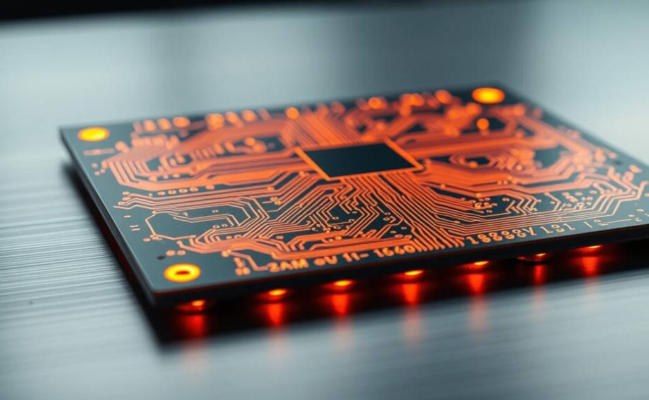
In PCB design, shape design not only determines the appearance of the product, but also affects the efficiency and cost of manufacturing and assembly. However, many customers often do not have high efficiency in PCB shape design after providing schematics, which leads to extended design cycles and even affects subsequent production.
Common Problems and Bottlenecks in PCB Shape Design
1. Unreasonable Size Planning– Ignoring parameters such as minimum spacing, minimum aperture, positive and negative tolerances, making it difficult for later production to meet requirements.
– The aspect ratio of the shape size is too large, which can easily cause PCB deformation, especially during reflow soldering or wave soldering.
2. Lack of Planning in Panel Design– The panel size does not fully consider the material utilization rate, wasting the board.
– No process edge is added to the special-shaped structure, affecting the efficiency of mounting and panel separation.
3. Insufficient Consideration of Mechanical Structure– Lack of Control over Board Thickness, Tolerance and Flatness, resulting in Impact on Component Performance.
– Ignoring Connector Layout and Space Reservation, resulting in Difficulties in Assembly and Heat Dissipation.
4. Insufficient communication of manufacturing requirements
– Ignoring communication with manufacturers, the design fails to fully adapt to production equipment and process limitations.
Practical suggestions for improving PCB appearance design efficiency;
1. Optimize the design process– Plan the size in advance: clarify the board utilization, processing technology requirements and installation requirements at the beginning of the design to avoid repeated modifications to the appearance design.
– Reserve process edges: design reasonable process edges for special-shaped structures to improve the operability of panel assembly and panel separation.
2. Use professional tools– CAD tool-assisted design: optimize the appearance design through software such as Altium Designer, KiCad, OrCAD, etc.
– For example, the Mechanical Layer function of Altium Designer can quickly verify whether the mechanical design is reasonable.
– 3D simulation and inspection: use the 3D simulation function to check the interference between the PCB and the shell to ensure the design adaptability.
3. In-depth communication with the manufacturer– Confirm the size, thickness, panel assembly method and equipment capacity with the manufacturer at the beginning of the design to ensure that the design meets the production requirements.
– Understand the advantages and disadvantages of V-cut, stamp hole and other panelization processes, and choose the best solution for different products.
4. Practical experience and feedback iteration– Summarize the success stories and failure lessons of past projects, and solidify the experience into design specifications.
– Regularly collect feedback from assembly teams and manufacturers to improve design processes and appearance optimization.