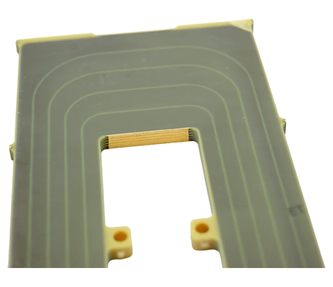
Heavy Copper PCBs-The "Powerhouse" of High-Power Electronics
In modern electronic devices, Heavy Copper PCBs act as a “powerhouse,” delivering stable power to high-current and high-power systems. Their defining feature lies in their significantly thicker copper layers compared to standard PCBs (typically ≥3 oz or 105μm for outer layers, with inner layers reaching up to 200 oz). This unique structure enables superior current-carrying capacity, efficient heat dissipation, and resistance to high temperatures.
Manufacturing Process: Precision Meets Innovation
Producing Heavy Copper PCBs requires overcoming traditional PCB limitations, primarily in material selection and advanced processing techniques
Material Requirements
- High-Tg laminates (e.g., Shengyi S1000-2M, Tg170) ensure minimal substrate deformation under high temperatures.
- High-purity electrolytic copper foil minimizes impurities that degrade conductivity
Core Techniques
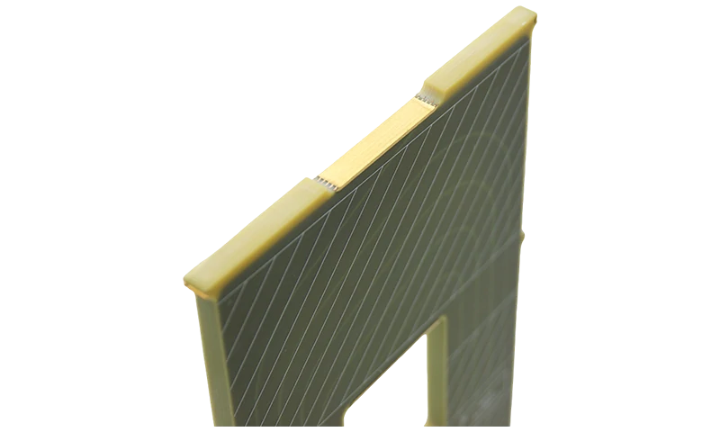
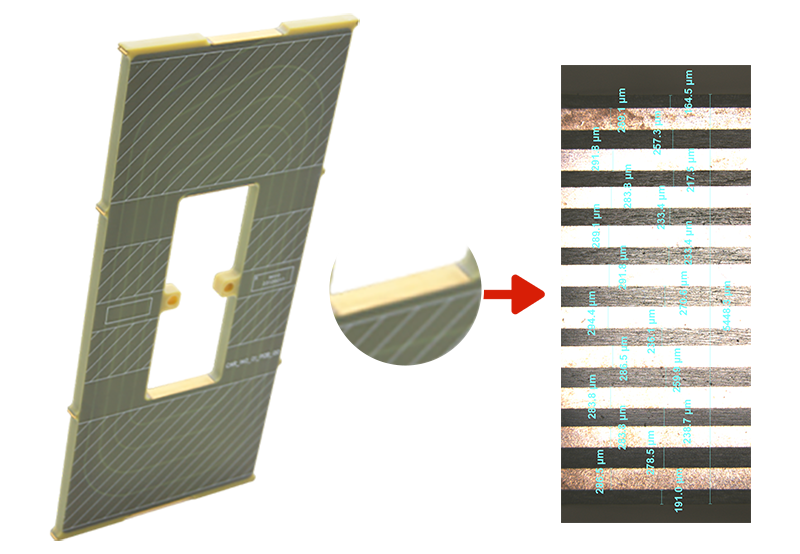
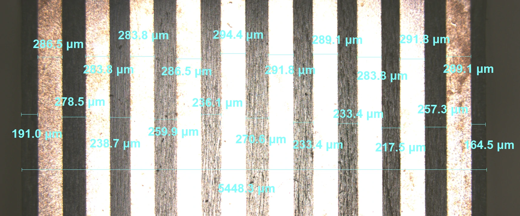
- Differential Etching: Dynamic adjustment of etchant concentration and flow rate prevents over-etching (sidewall erosion), maintaining precision (line width/spacing as low as 0.4mm/0.4mm).
- Multi-Stage Plating: A "plating-etching" cycle achieves localized copper thickness exceeding 20 oz, meeting extreme current demands.
- Thermal Design: Direct bonding of copper layers to heat sinks (e.g., TO-220 packages) improves thermal conductivity by 30%-50%.
Quality Assurance Rigorous testing includes thermal cycling (-40°C to 125°C), impedance verification, and thermal stress analysis to ensure long-term reliability.
Applications: From Consumer Tech to Aerospace
Heavy Copper PCBs are widely adopted across industries due to their performance
New Energy Vehicles
- Motor Controllers: Handle currents exceeding 100A for rapid charging/discharging.
- Battery Management Systems (BMS): Balance cell temperatures via thick copper layers, extending battery lifespan.
Industrial & Energy Systems
- Solar Inverters: Achieve >98% conversion efficiency, minimizing energy loss.
- Power Distribution Systems: Withstand voltages over 2000V, ensuring grid stability.
Communication & Computing
- 5G Base Station Power Modules: Support high-power RF signal transmission.
- AI Servers: 6 oz copper layers manage transient currents from CPUs/GPUs.
Aerospace
- Satellite Communication Modules: Endure extreme temperatures and radiation.
- Flight Control Systems: Enhanced mechanical strength prevents vibration-induced circuit fractures.
Technical Advantages & Future Trends
Key Benefits
- High Current Capacity: Each additional ounce of copper thickness increases current capacity by ~30%.
- Thermal Efficiency: Copper’s thermal conductivity (401 W/m·K) far exceeds aluminum, reducing component temperatures.
- Mechanical Durability: Thick copper layers boost connector lifespan (≥10,000 insertion cycles).
Challenges & Innovations
- Thermal Management: Embedded copper blocks and metal-core substrates (e.g., aluminum) optimize heat dissipation.
- Signal Integrity: Impedance control (±5% tolerance) reduces high-frequency signal loss.
Market Outlook The global Heavy Copper PCB market is projected to reach $478 million by 2033, growing at 8.49% CAGR, driven by renewable energy and AI computing demands.
Conclusion
As the “invisible backbone” of electronics, Heavy Copper PCBs are driving high-power devices toward miniaturization and efficiency. Innovations in manufacturing and materials will continue empowering smart vehicles, green energy, and other cutting-edge fields. With advancements in 3D stacking and optoelectronic integration, Heavy Copper PCBs may soon become a standard in next-generation electronics.