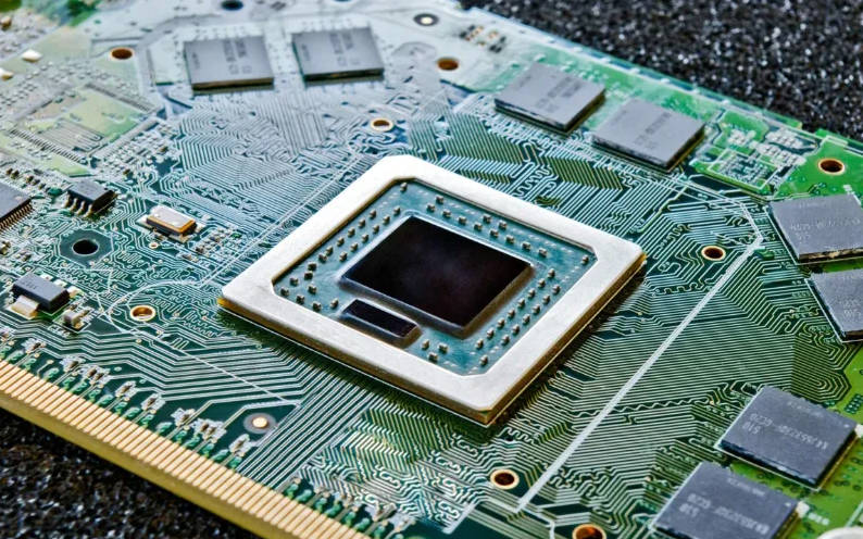
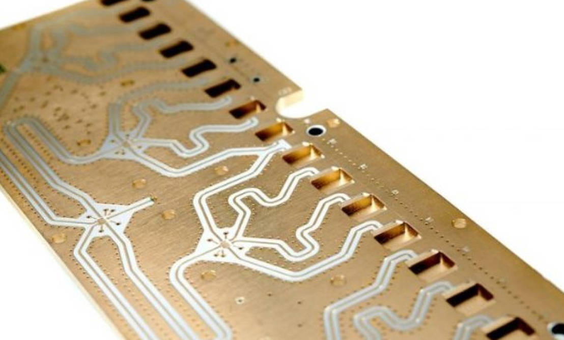
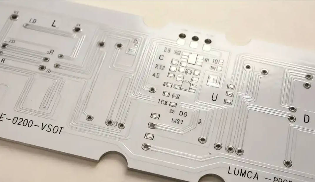
The primary difference between an HDI (High-Density Interconnect) PCB and a standard PCB lies in their circuit density and manufacturing complexity. HDI PCBs utilize microvias, thinner traces, and advanced fabrication techniques to pack significantly more functionality into a smaller, lighter board. In contrast, standard PCBs rely on larger, mechanically drilled through-hole vias and wider traces, making them simpler and more cost-effective for less demanding applications. This fundamental distinction impacts everything from performance and size to cost and application suitability.

Table of Contents
- Understanding the Basics: What is a Standard PCB?
- Introducing Advanced Technology: What is an HDI PCB?
- Key Technical Differences: A Head-to-Head Comparison
- Performance Implications: How Do They Stack Up?
- The Economic Equation: Cost vs. Capability
- Application Guide: When to Choose HDI vs. Standard PCBs?
- Summary: Key Takeaways in the HDI vs. Standard PCB Debate
- Frequently Asked Questions (FAQ)
Understanding the Basics: What is a Standard PCB?
A standard Printed Circuit Board, often called a conventional PCB, is the workhorse of the electronics industry. It forms the foundational platform for the vast majority of electronic devices that don’t require extreme miniaturization or ultra-high-speed performance. The defining characteristic of a standard PCB is its manufacturing process, which has been refined for decades to prioritize reliability and cost-effectiveness.
These boards are primarily built using a subtractive method where a full sheet of copper-clad laminate (most commonly FR-4) has unwanted copper etched away to leave the desired circuit traces. The most significant feature is the use of mechanically drilled through-hole vias. These holes pass through the entire thickness of the board, connecting all relevant layers. While effective, they are relatively large and consume valuable routing space on every layer they pass through, even those they don’t connect to. Trace and space widths on standard PCBs are typically 5 mils (0.127mm) or greater, limiting the overall component and routing density.
Introducing Advanced Technology: What is an HDI PCB?
HDI stands for High-Density Interconnect. As the name suggests, HDI PCBs are a more advanced class of circuit board designed to accommodate a higher number of interconnections in a smaller area. According to the IPC-2226 standard, a board is classified as HDI if its average number of electrical connections per square inch is significantly higher than a conventional board. This is achieved through a combination of sophisticated features and manufacturing processes.
The cornerstone of HDI technology is the microvia. These are tiny, laser-drilled holes, typically less than 6 mils (0.15mm) in diameter, that connect only adjacent layers. This frees up immense space on inner layers that would otherwise be occupied by large through-holes. HDI technology also enables finer lines and spaces (often 4 mils or less), smaller component pads, and the use of blind vias (connecting an outer layer to an inner layer) and buried vias (connecting two or more inner layers). These features work in concert to enable radical miniaturization and a dramatic increase in routing density, paving the way for compact and powerful devices like smartphones and wearables.
Key Technical Differences: A Head-to-Head Comparison
While both standard and HDI PCBs serve the same fundamental purpose—to connect electronic components—the way they achieve this is vastly different. Understanding these technical distinctions is crucial for any engineer or designer choosing between them.
Circuit Density and Trace/Space Width
The most apparent difference is the density of the circuitry. Standard PCBs are constrained by their larger features. With trace and space rules generally set at 5/5 mil (0.127mm) or wider, the ability to route signals between dense components like Ball Grid Arrays (BGAs) is limited. This often forces designers to add more layers to the board simply to find enough space for all the necessary connections, increasing board size and sometimes cost.
HDI PCBs shatter these limitations. By employing advanced imaging and etching processes, they can reliably achieve trace and space widths of 4/4 mil (0.100mm) or less. This, combined with smaller via pads, allows designers to route more traces in the same amount of space. The result is a much higher component density, allowing for more functionality to be packed into a smaller footprint, or for a complex design to be realized with fewer layers compared to a standard PCB approach.
Via Technology: Microvias vs. Through-Holes
The type of via used is perhaps the most critical differentiator. Standard PCBs almost exclusively use through-hole vias. These are drilled mechanically from the top to the bottom of the board. Their main drawback is their size and the fact that they create an “unwanted barrel” that blocks routing channels on all internal layers.
HDI PCBs leverage a portfolio of advanced via structures:
- Microvias: Laser-drilled vias that connect only one layer to its adjacent layer. Because they don’t pass through the whole board, they open up routing space on all other layers.
- Blind Vias: These connect an external layer to one or more internal layers but do not go all the way through the board.
- Buried Vias: These connect two or more internal layers and are completely invisible from the outside of the finished PCB.
- Via-in-Pad (VIP): A technique where the via is placed directly within the solder pad of a surface-mount component. This saves significant space and shortens signal paths, improving performance, and is a hallmark of HDI design.
Layer Count and Stack-up Complexity
While a standard PCB can have a high layer count (e.g., 16 or 20 layers), its construction is relatively simple. All layers are typically laminated together in a single pressing cycle. The stack-up is straightforward, with alternating core and prepreg materials.
HDI PCBs, on the other hand, are built using a process called Sequential Build-Up (SBU). This involves multiple lamination cycles. A central core is fabricated, then additional layers are added, drilled (with lasers for microvias), plated, and etched in sequence. This process is what allows for the creation of blind and buried vias. For example, a 1+N+1 stack-up means one HDI layer is added to each side of a conventional “core.” A 2+N+2 stack-up involves two sequential HDI layers on each side. This layered, sequential approach makes the manufacturing process more complex and time-consuming but is essential for achieving high density.
Size, Weight, and Form Factor
The direct consequence of higher density is miniaturization. Because HDI technology can fit the same number of components and connections into a much smaller area, the resulting PCBs are significantly smaller and lighter than their standard counterparts. A complex circuit that might require an 8-layer standard PCB could potentially be designed on a 6-layer HDI board with a smaller overall footprint. This reduction in size and weight is the primary driver for using HDI in portable electronics like smartphones, smartwatches, and medical monitoring devices.
Manufacturing Process and Materials
The manufacturing differences directly impact cost and lead time. Standard PCB fabrication relies on well-established, high-volume processes like mechanical drilling and single-cycle lamination, which are fast and inexpensive. The materials used are typically standard grades of FR-4.
HDI manufacturing is a more specialized and precise operation. It requires expensive laser drilling equipment for microvias, which can be either CO2 or UV lasers depending on the material. The sequential lamination process requires multiple steps of pressing, drilling, plating, and imaging, which increases both the time and cost of production. Furthermore, the high-performance demands of HDI often necessitate the use of more advanced, higher-cost laminate materials with better dielectric properties to support high-speed signals.
Performance Implications: How Do They Stack Up?
The differences between HDI and standard PCBs extend beyond physical dimensions; they have a profound impact on the electrical performance of the circuit.
Signal Integrity and Electrical Performance
For high-speed digital circuits or high-frequency RF applications, HDI offers a distinct performance advantage. The smaller via structures, particularly microvias, have significantly lower parasitic capacitance and inductance compared to large through-hole vias. This reduces signal reflections, distortion, and crosstalk, leading to superior signal integrity.
Furthermore, the ability to place components closer together and the shorter trace lengths possible on an HDI board reduce signal travel time and minimize the potential for EMI (Electromagnetic Interference) and RFI (Radio-Frequency Interference). The shorter stubs on blind vias, compared to the long unused barrel of a through-hole via, are critical for maintaining signal quality at gigabit speeds.
Power Delivery and Thermal Management
A robust Power Delivery Network (PDN) is crucial for modern high-current processors and FPGAs. HDI designs, with their use of microvias and via-in-pad technology, allow for more direct and lower-inductance paths from power planes to component power pins. This results in a more stable power supply with less voltage drop under load.
Thermally, the use of numerous microvias, especially when filled with conductive material, can create effective thermal pathways to draw heat away from hot components and dissipate it into internal ground or power planes. This improves the overall thermal management and reliability of the device without requiring bulky external heatsinks.
The Economic Equation: Cost vs. Capability
There is no question that on a per-board basis, an HDI PCB is more expensive to manufacture than a standard PCB of the same size and layer count. The specialized equipment, complex processes, and tighter tolerances all contribute to a higher unit price. However, a simple unit cost comparison can be misleading.
One must consider the Total Cost of Ownership (TCO). An HDI design might allow an 8-layer board to be condensed into a 6-layer board, potentially offsetting some of the technology premium. More importantly, if miniaturization is a key product requirement, the higher cost of the HDI PCB may enable a smaller, more desirable, and ultimately more profitable final product. The improved electrical performance might also eliminate the need for other expensive signal-conditioning components on the board. The decision is a trade-off between the upfront manufacturing cost and the value delivered through performance, size, and reliability.
| Feature | Standard PCB | HDI PCB |
|---|---|---|
| Via Type | Through-Hole (Mechanical Drill) | Microvias, Blind/Buried Vias (Laser Drill) |
| Trace/Space Width | ≥ 5 mil (0.127mm) | ≤ 4 mil (0.100mm), often finer |
| Component Density | Lower | Significantly Higher |
| Lamination Process | Single Cycle | Sequential Build-Up (Multiple Cycles) |
| High-Speed Performance | Good for moderate speeds | Excellent due to shorter paths and smaller vias |
| Form Factor | Larger, Heavier | Smaller, Lighter |
| Manufacturing Cost | Lower | Higher |
Application Guide: When to Choose HDI vs. Standard PCBs?
Choosing the right PCB technology is a critical design decision that balances cost, performance, and physical constraints. Here’s a practical guide to help you decide.
When is a Standard PCB the Right Choice?
Standard PCBs remain the ideal choice for a wide range of applications where cost is a primary driver and space is not the main constraint. Their reliability and simple manufacturing process make them a safe and economical option.
- Prototypes and Hobby Projects: The low cost and fast turnaround times make standard boards perfect for initial testing and personal projects.
- Simple Consumer Electronics: Devices like kitchen appliances, toys, and remote controls do not require the density of HDI.
- Industrial Control Systems: In applications where space is plentiful and the environment is rugged, larger components and traces on a standard board can be more robust.
- Power Supplies and LED Lighting: These applications often prioritize thermal dissipation and current-carrying capacity over miniaturization, which a well-designed standard board can handle effectively.
When Should You Invest in HDI Technology?
Investing in HDI becomes necessary when product requirements push beyond the capabilities of conventional boards. If your design involves any of the following, HDI is likely the correct path.
- Miniaturization is Key: For any product that needs to be small and lightweight, such as smartphones, wearables, tablets, and compact medical devices.
- High-Speed Signals: When dealing with high-speed processors, memory interfaces (like DDR4/5), or high-frequency communication protocols (5G, Wi-Fi 6), the superior signal integrity of HDI is often a requirement.
- Dense, High Pin-Count Components: Modern FPGAs and processors with fine-pitch BGA packages (e.g., 0.5mm pitch or less) are nearly impossible to route effectively on a standard PCB without an excessive number of layers. HDI’s via-in-pad and microvia technologies are essential here.
- Complex, Feature-Rich Devices: Products that integrate numerous functions—like a car’s infotainment and advanced driver-assistance system (ADAS)—rely on HDI to fit all the necessary electronics into a confined space.
Summary: Key Takeaways in the HDI vs. Standard PCB Debate
The choice between HDI and standard PCBs is a strategic engineering decision. A standard PCB offers a proven, cost-effective solution for a huge array of electronics. Its strengths lie in simplicity, reliability for non-dense designs, and low manufacturing cost. An HDI PCB, in contrast, is a specialized, high-performance solution that trades higher upfront cost and complexity for unparalleled advantages in miniaturization, circuit density, and electrical performance. It is the enabling technology behind today’s most advanced and compact electronic devices.
Frequently Asked Questions (FAQ)
Is designing an HDI PCB more difficult than a standard PCB?
Yes, it is significantly more complex. HDI design requires a deep understanding of microvia structures, sequential lamination, controlled impedance, and signal integrity. It also necessitates advanced PCB design software with features specifically for HDI routing and rule-checking.
What is the main reason companies switch from standard to HDI PCBs?
The primary driver is almost always miniaturization. The need to create smaller, lighter, and more portable products with increasing functionality forces designers to adopt the higher density offered by HDI technology. Improved electrical performance for high-speed circuits is a close second.
Can I use a standard PCB for a design with a BGA component?
Yes, but with limitations. Standard PCBs can typically handle BGAs with a pitch of 1.0mm or greater. For BGAs with a finer pitch (e.g., 0.8mm, 0.5mm), routing all the signals becomes extremely difficult or impossible without resorting to HDI techniques like via-in-pad and microvias.
HDI PCB, Standard PCB, HDI PCB vs Standard PCB, Microvia, Through-hole via, PCB technology, High-Density Interconnect, PCB design, difference between HDI and standard PCB, when to use HDI PCB, PCB manufacturing process, circuit density, via-in-pad, sequential build-up, PCB cost, signal integrity, electronic manufacturing


