Unlocking Complexity: How Advanced PCB Tools Master Multilayer and HDI Designs
Advanced PCB design tools are essential for creating modern multilayer and High-Density Interconnect (HDI) boards, supporting engineers by providing an integrated environment that masterfully handles complexity. Key features include intelligent layer stack managers for precise material and impedance control, sophisticated routing engines capable of handling microvias and high-speed signals, built-in signal and power integrity (SI/PI) analysis to prevent errors before fabrication, and powerful, constraint-driven design rule checking (DRC) that goes far beyond simple spacing rules. These synergistic capabilities transform the design process from a manual layout task into a holistic engineering discipline, enabling the creation of the compact, powerful electronics that define today’s technology.

Table of Contents
- What Defines a Multilayer or HDI PCB? A Quick Primer
- The Core Pillars: How Modern EDA Software Tames Complexity
- A Practical Walkthrough: Designing an HDI Board with Advanced Tools
- Why Legacy Tools Falter with Modern PCB Designs
- Which Advanced PCB Tools Lead the Pack?
- The Future of PCB Design: What’s Next for Multilayer and HDI Tools?
- Conclusion: More Than Just a Layout Tool
What Defines a Multilayer or HDI PCB? A Quick Primer
Before diving into the software solutions, it’s crucial to understand the problems they solve. The evolution from simple, single-sided boards to complex, high-performance designs necessitated a complete overhaul of design methodologies and the tools that support them. This progression is marked by two key milestones: the adoption of multilayer boards and the advent of HDI technology.
The Leap from Single-Layer to Multilayer PCBs
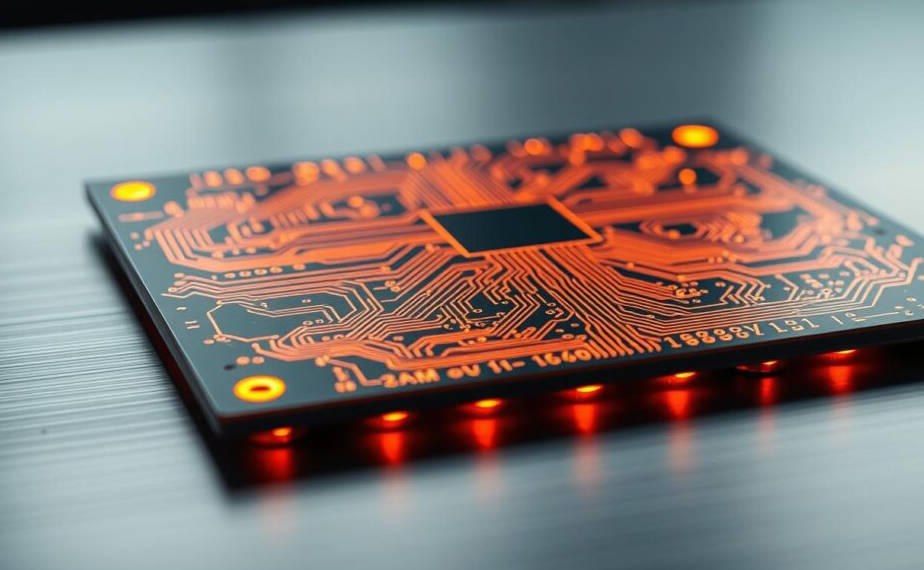
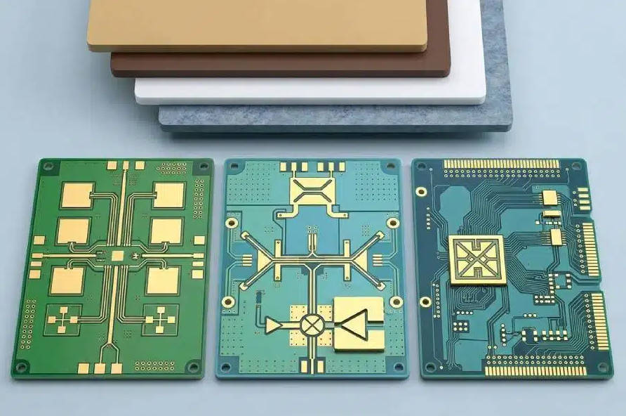
A multilayer PCB is a printed circuit board that has more than two layers of conductive copper foil. These boards are created by laminating several double-sided or single-sided boards together with insulating layers in between. The primary driver for this evolution was the need for increased circuit density and the ability to manage complex routing. By adding internal layers, designers gained dedicated planes for power and ground, which drastically improved power distribution and reduced electromagnetic interference (EMI). This structure also provided more space for signal routing, allowing for smaller board sizes and more intricate connections without resorting to a web of convoluted traces on the outer layers.
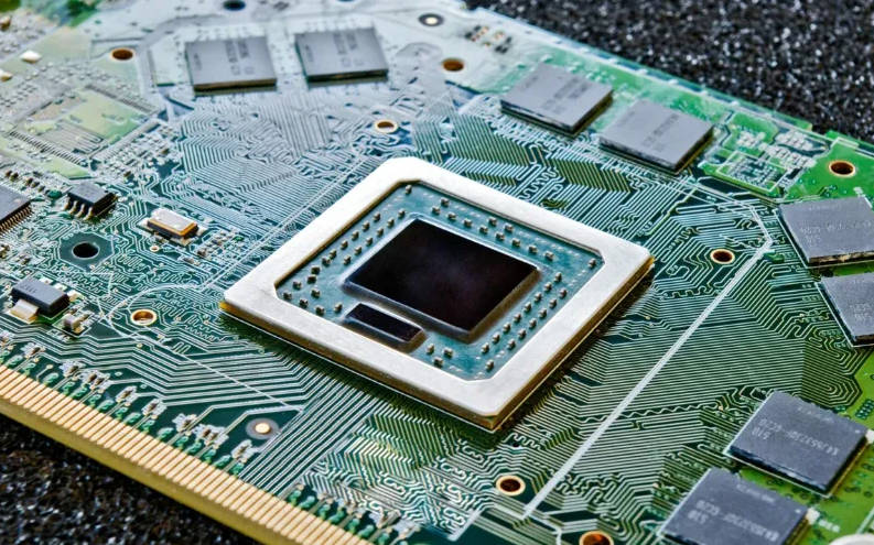
The HDI Revolution: Pushing the Boundaries of Density
High-Density Interconnect (HDI) technology takes the multilayer concept to the next level. HDI PCBs are characterized by finer lines and spaces, smaller vias (often microvias), and higher connection pad density. The goal of HDI is to pack more functionality into an even smaller area, which is critical for devices like smartphones, wearables, and advanced computing modules. This is achieved through advanced features like blind and buried vias, which only connect specific layers, and via-in-pad technology, which allows components to be placed directly on top of vias. This frees up significant surface area that would otherwise be used for traditional via pads and fanout traces.
The Core Pillars: How Modern EDA Software Tames Complexity
Modern Electronic Design Automation (EDA) software isn’t just a drawing tool; it’s a sophisticated engineering platform. It addresses the challenges of multilayer and HDI designs through a set of integrated, intelligent features that work in concert. These can be understood as five core pillars of support.
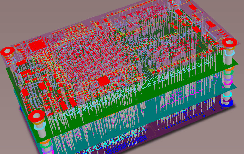
Pillar 1: The Intelligent Layer Stack Manager – The Board’s Digital Twin
The foundation of any multilayer or HDI design is its layer stackup. Advanced PCB tools feature a dedicated Layer Stack Manager that acts as a digital twin of the physical board. This is far more than a simple list of layers. Here, engineers can precisely define every aspect of the stackup, including the thickness and dielectric constant (Dk) of each core and prepreg material. The software uses this information to power an integrated field solver, allowing for the creation of precise impedance profiles. A designer can specify a target impedance, like 50 ohms for a single-ended trace or 90 ohms for a USB differential pair, and the tool will automatically calculate the required trace width for that specific layer, saving countless hours of manual calculation and preventing signal integrity issues.
Pillar 2: Sophisticated Routing Engines for Dense Environments
Routing a dense HDI board is impossible without specialized tools. Modern routing engines are built to handle the unique structures of these designs. This includes native support for:
- Microvias, Blind Vias, and Buried Vias: The software understands the manufacturing process for these structures. It allows designers to define via spans across specific layers (e.g., from Layer 1 to 2 for a blind via) and enforces rules to prevent invalid combinations. This includes managing stacked and staggered microvia configurations, which are common in high-pin-count BGA breakouts.
- Via-in-Pad Designs: Advanced tools support placing vias directly within the solder pads of a component. They manage the necessary design rules and output the specific fabrication data needed for the processes that fill and plate over these vias to ensure a reliable solder connection.
- Controlled Impedance and Differential Pair Routing: When routing a high-speed differential pair, the software actively maintains the specified trace width and gap throughout the entire length of the traces. It can automatically adjust for routing around obstacles and ensure length matching to prevent signal skew, a critical factor for interfaces like DDR memory and PCIe.
Pillar 3: Integrated Simulation and Analysis (SI/PI)
In the past, signal integrity (SI) and power integrity (PI) analysis were post-design processes, often performed by a separate specialist. This was slow and inefficient. Advanced PCB tools now integrate simulation engines directly into the layout environment. As an engineer routes a critical high-speed trace, they can immediately run a simulation to check for impedance discontinuities, reflections, or excessive crosstalk from neighboring signals. Similarly, Power Integrity tools allow for the analysis of the Power Delivery Network (PDN). Designers can visualize voltage drops and high current density areas on their power planes, allowing them to add necessary decoupling capacitors or thicken copper pours before the design is ever sent to manufacturing, preventing costly respins.
Pillar 4: Constraint-Driven Design and Advanced DRC
The concept of Design Rule Checking (DRC) has evolved significantly. In modern tools, it’s part of a larger constraint-driven design methodology. Instead of just checking for simple clearances at the end, the engineer defines a complex set of rules and constraints at the beginning of the project. These rules can be assigned to specific nets, groups of nets (net classes), or defined physical regions of the board. For example, a rule can specify that all DDR4 address lines must be routed on Layer 3, have a 40-ohm impedance, and be length-matched to within 2mm of each other. The layout tool’s online DRC then acts as a guide, preventing the designer from violating these rules in real-time and highlighting any existing errors, ensuring the design is “correct by construction.”
Pillar 5: 3D Visualization and MCAD-ECAD Co-Design
PCBs do not exist in a vacuum; they must fit inside a mechanical enclosure. Advanced tools provide a real-time, photo-realistic 3D view of the board, including components, copper, and silkscreen. This is invaluable for multilayer designs, as it helps visualize component clearances and complex assembly details. More importantly, these tools offer seamless MCAD-ECAD co-design. An electrical engineer can import a 3D model of the enclosure from a mechanical tool like SolidWorks, design the board within its constraints, and then export the finished PCB back to the mechanical engineer. This bidirectional data exchange ensures that the board fits perfectly on the first try, eliminating physical prototype errors related to mounting holes, connector positions, and component height restrictions.
A Practical Walkthrough: Designing an HDI Board with Advanced Tools
To illustrate how these pillars work together, consider the workflow for breaking out a fine-pitch Ball Grid Array (BGA) component on an HDI board. First, the engineer uses the Layer Stack Manager to define an 8-layer stackup with two HDI layers on the top and bottom. Next, within the Constraint Manager, they set up rules for the BGA, defining microvia types for the inner pins and specific trace widths for different signal groups. As they begin routing, the interactive router automatically suggests fanout patterns using via-in-pad for the ground pins and microvias for the signals. While routing a high-speed interface, the Differential Pair Router keeps the traces perfectly coupled. Periodically, the engineer runs an in-design SI simulation to check for reflections. Finally, they switch to the 3D view to confirm that a tall capacitor near the BGA doesn’t interfere with the enclosure. This entire process is guided and validated by the software at every step.
Why Legacy Tools Falter with Modern PCB Designs
Older or lower-tier PCB design tools simply lack the integration and intelligence needed for multilayer and HDI work. Their layer management is often just a list of layers with no concept of materials or impedance. Routing is a manual process, with no built-in awareness of differential pairs or length matching. They lack integrated SI/PI analysis, forcing a “design and hope” approach. Their DRC systems are basic, only capable of checking simple spacing rules and unable to manage the complex, high-speed constraints that define modern electronics. Attempting an HDI design with such a tool would be an exercise in extreme frustration, likely resulting in a non-functional board that is impossible to manufacture.
Which Advanced PCB Tools Lead the Pack?
The market for high-end EDA software is dominated by a few key players, each offering a powerful suite of tools tailored for complex designs. While feature sets are competitive, they often have different strengths and user interfaces.
| EDA Software Suite | Key Strengths for Multilayer/HDI Design | Primary User Base |
|---|---|---|
| Altium Designer | Unified design environment, intuitive 3D engine, excellent layer stack management, and a strong user community. Widely praised for its ease of use. | Small-to-medium businesses, startups, and individual professionals. |
| Cadence Allegro / OrCAD | Extremely powerful constraint manager, best-in-class SI/PI analysis (Sigrity), and robust team collaboration features. Considered an industry standard for high-speed design. | Large enterprises, semiconductor companies, and high-end engineering teams. |
| Siemens EDA (Mentor) Xpedition | Deep integration with the entire Siemens ecosystem (including MCAD), powerful concurrent design capabilities, and advanced DFM analysis. | Aerospace, automotive, and large-scale enterprise environments. |
| Zuken CR-8000 | Strong focus on system-level and co-design (chip, package, board), excellent 3D platform, and powerful tools for managing design variants and constraints. | Automotive, industrial, and complex system design companies. |
The Future of PCB Design: What’s Next for Multilayer and HDI Tools?
The evolution of PCB design software is far from over. The next frontier involves leveraging artificial intelligence and machine learning to assist in complex tasks. Imagine AI-powered routers that can intelligently route an entire dense BGA in seconds, optimizing for both signal integrity and manufacturability based on thousands of previous designs. We are also seeing a push towards deeper cloud integration for seamless collaboration among globally distributed teams and tighter, real-time links to manufacturer capabilities. This “digital thread” will connect the design tool directly to the factory floor, allowing for instant DFM feedback and a more streamlined production process.
Conclusion: More Than Just a Layout Tool
In conclusion, advanced PCB tools support multilayer and HDI designs by moving beyond the role of a simple layout editor. They have become comprehensive engineering ecosystems that provide designers with the intelligent layer management, sophisticated routing capabilities, integrated analysis, and constraint-driven validation necessary to tackle the immense challenges of modern electronics. By unifying these functions into a single environment, these tools empower engineers to innovate with confidence, creating the smaller, faster, and more powerful devices that will shape our future.
Advanced PCB tools, Multilayer PCB design, HDI design, PCB design software, How do PCB tools support HDI design?, features for multilayer PCB design, managing layer stackup, signal integrity analysis, microvia and via-in-pad design, design rule checking for complex PCBs, EDA tools, high-density interconnect