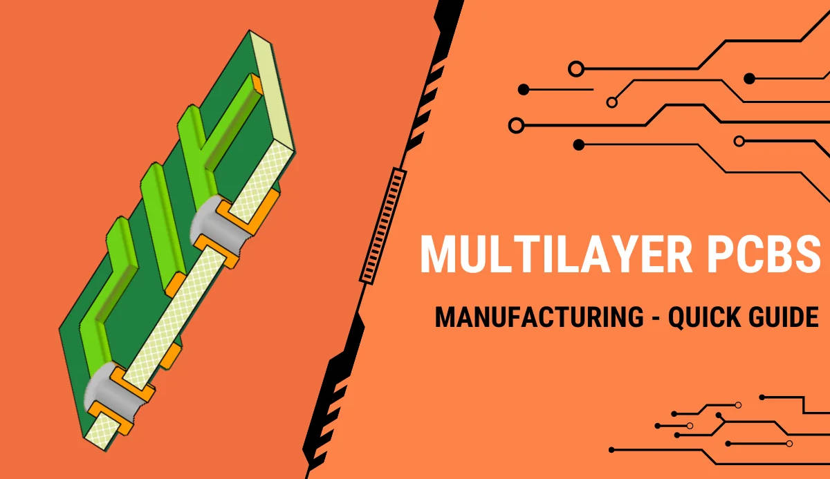
A Comprehensive Guide to the Multilayer PCB Fabrication Process
The multilayer PCB fabrication process is a sophisticated manufacturing sequence used to create printed circuit boards with three or more conductive copper layers laminated together with insulating material. This intricate process involves a series of steps including inner layer imaging, lamination, drilling, plating, and outer layer processing to build a compact, high-density circuit board essential for advanced electronics. Unlike simpler single or double-sided boards, multilayer fabrication requires extreme precision to ensure proper alignment and electrical connectivity between all the buried and external layers.
Table of Contents
- What is a Multilayer PCB?
- Why Choose a Multilayer Design Over Single or Double-Sided?
- The Core Components: Materials Used in Multilayer PCBs
- The Step-by-Step Multilayer PCB Fabrication Process
- Step 1: Design Review and DFM Check
- Step 2: Inner Layer Imaging and Etching
- Step 3: Automated Optical Inspection (AOI) of Inner Layers
- Step 4: Lamination – Fusing the Layers Together
- Step 5: Drilling – Creating Vias and Holes
- Step 6: Deburring and Hole Cleaning
- Step 7: Copper Deposition and Plating
- Step 8: Outer Layer Imaging and Etching
- Step 9: Solder Mask Application
- Step 10: Silkscreen (Legend) Printing
- Step 11: Surface Finish Application
- Step 12: Electrical Testing (E-Test)
- Step 13: Depanelization and Final Inspection
- Key Challenges in Multilayer PCB Manufacturing
- Frequently Asked Questions (FAQ)
- Conclusion
What is a Multilayer PCB?
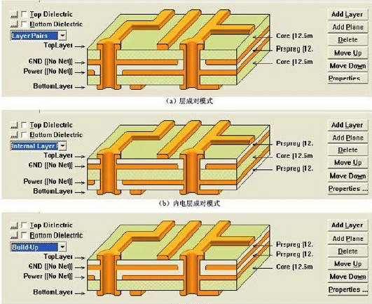
A multilayer Printed Circuit Board (PCB) is a circuit board comprised of more than two conductive layers, typically made of copper. These layers are stacked vertically with insulating material, known as prepreg and core, separating them. The layers are interconnected through drilled holes called vias, which are plated with copper to create electrical pathways. This layered construction allows for much more complex and dense circuit designs compared to single or double-sided PCBs, making them the backbone of sophisticated electronic devices like smartphones, computers, medical equipment, and automotive systems.
Why Choose a Multilayer Design Over Single or Double-Sided?
The decision to use a multilayer PCB is driven by the need for increased functionality and reduced size. Single and double-sided boards are limited in routing space, which restricts circuit complexity. Multilayer boards overcome this by providing dedicated internal layers for power (VCC) and ground (GND) planes, which significantly improves signal integrity by reducing electromagnetic interference (EMI) and providing stable voltage distribution. Furthermore, they allow for a much higher component density, enabling engineers to create smaller, lighter, and more powerful products.
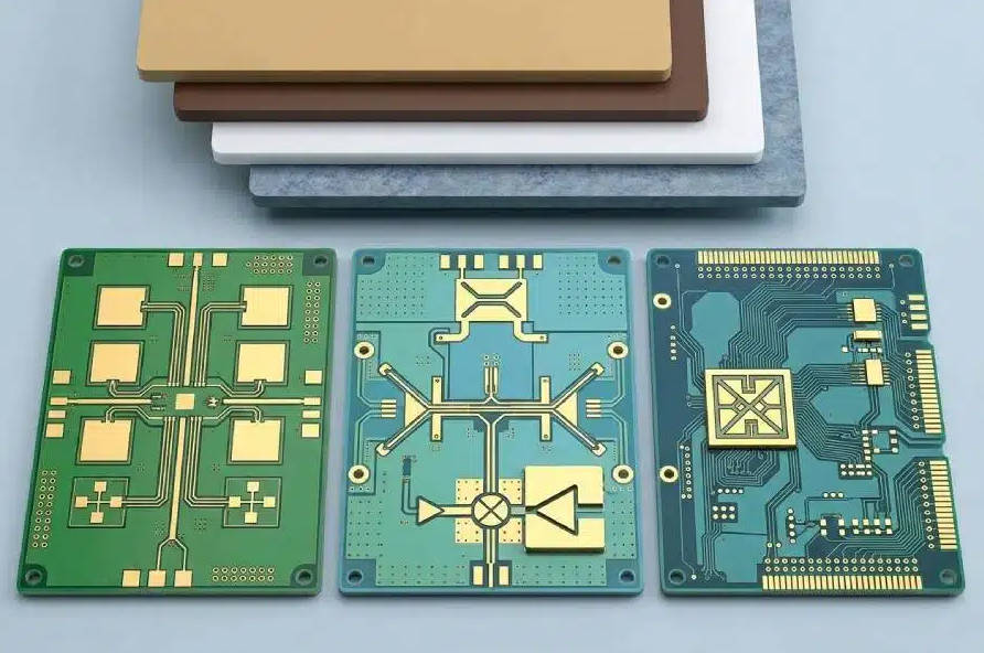
The Core Components: Materials Used in Multilayer PCBs
Understanding the fabrication process begins with knowing the fundamental materials. Each material plays a critical role in the board’s structural integrity, electrical performance, and thermal resistance. The primary materials are carefully selected based on the application’s requirements.
| Material | Role in the PCB | Key Properties |
|---|---|---|
| Core (Substrate) | The foundational rigid base for the inner layers. Typically a sheet of FR-4 with copper foil laminated on one or both sides. | Provides mechanical strength and electrical insulation. FR-4 (Flame Retardant 4) is the industry standard. |
| Copper Foil | The conductive material that forms the traces, pads, and planes of the circuit. | High electrical conductivity. Thickness is measured in ounces per square foot (e.g., 1 oz, 2 oz). |
| Prepreg | A woven glass cloth pre-impregnated with epoxy resin. It acts as the “glue” during lamination. | When heated, the resin flows, fills gaps, and bonds the core layers and copper foil together, then cures to form a solid insulator. |
| Solder Mask | A protective polymer coating applied to the outer layers of the PCB. | Insulates copper traces from accidental contact, prevents solder bridges during assembly, and protects against oxidation. |
| Silkscreen (Legend) | The ink layer used to print component designators, logos, and other markings on the board. | Aids in manual and automated component placement and debugging. |
The Step-by-Step Multilayer PCB Fabrication Process
The manufacturing of a multilayer PCB is a precise, sequential process where each step builds upon the last. A single mistake at an early stage, especially on an inner layer, cannot be corrected later and will result in a scrapped board. This unforgiving nature is why quality control is paramount throughout the workflow.
Step 1: Design Review and DFM Check
Before any physical manufacturing begins, the customer’s design files (typically in Gerber or ODB++ format) undergo a thorough review. Engineers perform a Design for Manufacturability (DFM) check to identify potential issues that could impact production yield or board reliability. This analysis ensures that trace widths, spacing, hole sizes, and layer stack-up conform to the manufacturer’s capabilities, preventing costly errors down the line.
Step 2: Inner Layer Imaging and Etching
The process starts with the inner layers. A sheet of copper-clad core material is cleaned and then coated with a light-sensitive film called photoresist. The circuit pattern for the layer is transferred onto the photoresist using a laser direct imaging (LDI) system or a phototool (film) and UV light. The light hardens the resist, protecting the copper that will form the circuit traces. The board is then submerged in a chemical solution that etches away the unprotected, unhardened copper, leaving behind the desired circuit pattern. The remaining photoresist is then stripped off.
Step 3: Automated Optical Inspection (AOI) of Inner Layers
This is a critical quality control step. Since the inner layers will be inaccessible after lamination, they must be perfect. Each etched inner layer is scanned by an Automated Optical Inspection (AOI) machine. This machine uses high-resolution cameras to compare the etched layer against the original design data, flagging any defects such as shorts (unwanted copper connections), opens (broken traces), or incorrect spacing. Any defective layers are discarded at this stage.
Step 4: Lamination – Fusing the Layers Together
Lamination is the core process that defines a multilayer PCB. The verified inner layer cores are stacked together with alternating layers of prepreg. A sheet of copper foil is typically placed on the top and bottom of the stack to form the outer layers. This entire “book” is placed in a large lamination press. Under immense pressure and high temperature, the epoxy resin in the prepreg melts, flows, and cures, bonding all the layers into a single, solid, inseparable board.
Step 5: Drilling – Creating Vias and Holes
Once the layers are laminated, holes must be drilled to connect them electrically and to mount components. A computer-controlled drilling machine uses the design files to accurately drill holes, known as vias, through-holes, and mounting holes. For extremely small or high-density vias (microvias), laser drilling may be used. The precision of this step is vital, as any misalignment can ruin the electrical connections between layers.
Step 6: Deburring and Hole Cleaning
After drilling, small burrs of copper may remain around the edges of the holes, and resin smear can coat the inner walls. The board undergoes a deburring process to remove these imperfections. Subsequently, a chemical and plasma cleaning process is used to thoroughly clean the inside of the drilled holes, ensuring a clean copper surface is exposed on each inner layer for proper plating.
Step 7: Copper Deposition and Plating
To make the non-conductive walls of the drilled holes conductive, a very thin layer of copper is deposited over the entire board surface, including inside the holes. This is done through a chemical process called electroless copper deposition. This initial layer is too thin for reliable current flow, so it is reinforced through electrolytic plating (electroplating), where the board is submerged in a plating bath and an electric current deposits a thicker, more robust layer of copper in the holes and on the outer surfaces.
Step 8: Outer Layer Imaging and Etching
This step is similar to inner layer imaging, but the goal is slightly different. Photoresist is applied to the outer layers, and the circuit pattern is exposed. The subsequent plating process (often a tin-lead alloy) is applied only to the areas that will become the final circuit. This plated material acts as an etch resist. The board is then placed in an etching solution that removes the unwanted copper, leaving only the traces and pads protected by the tin-lead plating. The resist is then stripped away.
Step 9: Solder Mask Application
The iconic green (or other color) coating is now applied. The entire board is covered with a solder mask ink. Using a photolithography process, the areas where components will be soldered (the pads) are exposed and the mask is cured with UV light. The unexposed mask is washed away, leaving the copper pads bare while protecting all other traces from oxidation and preventing solder bridges during assembly.
Step 10: Silkscreen (Legend) Printing
Next, reference designators, component outlines, company logos, and other markings are printed onto the board’s surface. This is typically done using an inkjet printing process that applies a non-conductive epoxy ink. The silkscreen provides a vital human-readable guide for assembly and testing.
Step 11: Surface Finish Application
The exposed copper pads where components will be soldered are highly susceptible to oxidation. To protect them and ensure good solderability, a surface finish is applied. Common finishes include HASL (Hot Air Solder Leveling), ENIG (Electroless Nickel Immersion Gold), Immersion Silver, and OSP (Organic Solderability Preservative). The choice of finish depends on the application, cost, and component type.
Step 12: Electrical Testing (E-Test)
Every single multilayer PCB must undergo a final electrical test to verify its integrity. Two primary methods are used:
- Bed of Nails Testing: A fixture with dozens or hundreds of spring-loaded pins makes contact with test points on the board to check for continuity (connections that should exist) and isolation (shorts between nets that shouldn’t).
- Flying Probe Testing: Two or more robotic probes move around the board, testing pairs of points programmatically. It’s slower but requires no custom fixture, making it ideal for prototypes and small batches.
Step 13: Depanelization and Final Inspection
PCBs are often manufactured in large panels containing multiple copies of the same board. In the final step, these individual boards are separated from the panel. This can be done by routing (milling) or V-scoring (cutting a V-shaped groove for easy snapping). After separation, each board undergoes a final visual inspection for any cosmetic defects before being vacuum-sealed and shipped.
Key Challenges in Multilayer PCB Manufacturing
The complexity of multilayer PCBs introduces unique manufacturing challenges that require advanced technology and rigorous process control.
- Layer-to-Layer Registration: Ensuring all layers align perfectly is the biggest challenge. Even minute shifts during lamination can cause drilled vias to miss their intended pads on inner layers, resulting in open circuits.
- Impedance Control: For high-speed digital circuits, the impedance of traces must be tightly controlled. This requires precise management of trace width, dielectric thickness, and material properties throughout the process.
- Drilling and Plating Aspect Ratio: Drilling and successfully plating copper through very small holes in a thick board (a high aspect ratio) is difficult. It requires specialized equipment to ensure complete, uniform plating inside the via barrel.
- Thermal Stress: The lamination process involves high temperatures and pressures. Different materials expand and contract at different rates, which can induce stress and cause board warpage if not managed properly.
Frequently Asked Questions (FAQ)
What is the difference between core and prepreg?
A core is a rigid sheet of cured FR-4 with copper foil already laminated to it, forming a self-contained double-sided board. Prepreg is a flexible, uncured sheet of fiberglass impregnated with resin that acts as an adhesive and insulator between core layers during lamination.
How many layers can a multilayer PCB have?
While 4 to 12 layers are most common for consumer and industrial electronics, multilayer PCBs can theoretically have over 100 layers for extremely complex applications like high-end servers, aerospace, and defense systems.
What is a via in a multilayer PCB?
A via is a copper-plated hole that provides an electrical connection between different layers of the board. There are different types, including through-hole vias (go through the entire board), blind vias (connect an outer layer to one or more inner layers), and buried vias (connect two or more inner layers without reaching an outer layer).
Conclusion
The multilayer PCB fabrication process is a testament to modern engineering and chemical precision. It transforms a digital design into a highly integrated physical component that powers nearly every piece of advanced technology we use. From the initial DFM check to the final electrical test, each step is meticulously controlled to manage the immense complexity of stacking and interconnecting multiple circuit layers. Understanding this workflow not only demystifies how complex electronics are made but also highlights the critical importance of quality, precision, and expertise in producing reliable, high-performance circuit boards.
Multilayer PCB fabrication process, How multilayer PCBs are made, Multilayer PCB manufacturing, Printed Circuit Board fabrication, What are the steps in multilayer pcb fabrication?, Multilayer pcb lamination process, Inner layer vs outer layer pcb processing, PCB via drilling and plating, FR-4 prepreg and core materials, Automated Optical Inspection (AOI) in pcb, Multilayer circuit board construction, PCB manufacturing steps, DFM check for pcb, Solder mask application process, What is a multilayer pcb