Deciding between a multilayer PCB and a 3D PCB involves choosing between established planar density and innovative spatial integration. A multilayer Printed Circuit Board (PCB) is the best choice for complex, high-density electronic products with a conventional flat form factor, offering proven reliability and cost-effective scaling. In contrast, a 3D PCB, or 3D-Molded Interconnect Device (3D-MID), is ideal for products where space is minimal, the shape is non-conventional, and the electronic circuitry must be integrated directly onto the surface of a three-dimensional component, such as in wearables, medical implants, and advanced sensors.
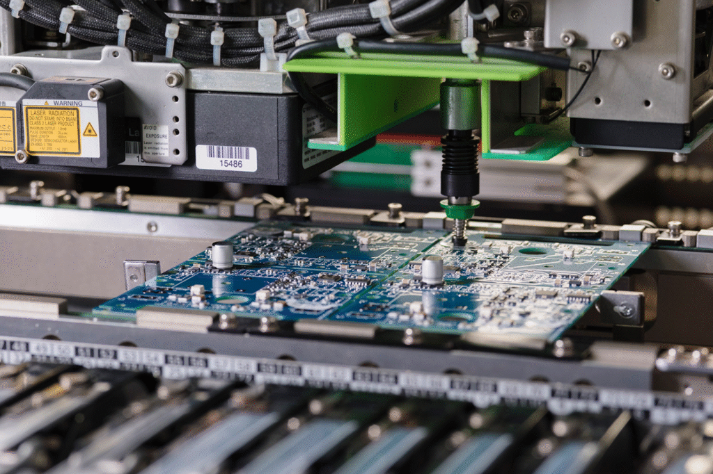
Table of Contents
- What is a Multilayer PCB? A Deep Dive into Layered Electronics
- What is a 3D PCB? Exploring the Third Dimension in Circuitry
- Head-to-Head Comparison: Multilayer PCB vs. 3D PCB
- How to Decide? Key Factors for Your Product’s Success
- The Future of Circuit Design: Are 3D PCBs the Next Big Thing?
- Conclusion: Making the Right Choice for Innovation and Functionality
What is a Multilayer PCB? A Deep Dive into Layered Electronics
A multilayer PCB is an electronic circuit board composed of more than two conductive copper layers. Think of it as a multi-story building for electronics; rather than expanding outwards, it builds upwards, stacking layers of circuits on top of one another. These layers are laminated and bonded together with insulating materials (prepreg) and a core, creating a single, robust board. This layered approach is the backbone of modern electronics, enabling engineers to create incredibly complex and dense circuits within a defined footprint.
The Fundamental Structure: Stacking Layers for Complexity
The core concept of a multilayer PCB is the vertical integration of circuit layers. A simple double-sided board has a top and bottom layer. A 4-layer board, a common starting point for multilayer designs, typically includes a top signal layer, a ground plane, a power plane, and a bottom signal layer. This structure is critical for high-speed digital designs, as dedicated power and ground planes provide excellent signal integrity by minimizing noise, crosstalk, and electromagnetic interference (EMI). As device complexity increases, boards can scale to 6, 8, 12, or even 100+ layers, accommodating thousands of components and tens of thousands of connections in devices like servers, smartphones, and advanced computing hardware.
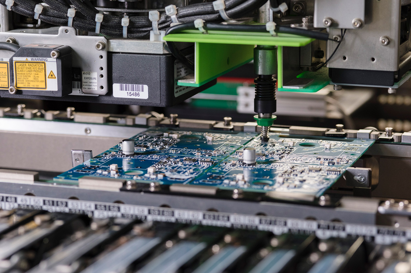
How are Multilayer PCBs Manufactured? The Lamination Process
The fabrication of a multilayer PCB is a precise and established process. It begins with the creation of individual inner-layer cores, which are essentially thin, double-sided PCBs. These cores are etched with the desired circuit patterns. Next, these etched cores are stacked together with layers of “prepreg,” an epoxy-impregnated fiberglass material that acts as a glue and insulator. The stack-up is then placed in a lamination press, where immense pressure and high temperature are applied. This process cures the epoxy in the prepreg, bonding all the layers into a single, inseparable board. Following lamination, holes (vias) are drilled through the board to connect the different layers, which are then plated with copper to create electrical pathways.
Key Advantages and Common Applications
The primary advantage of multilayer PCBs is their ability to achieve extraordinary circuit density. This makes them indispensable for almost all sophisticated electronics. Other key benefits include improved signal integrity due to controlled impedance and dedicated power/ground planes, smaller overall size for a given functionality compared to single-layer boards, and enhanced durability. Consequently, you will find multilayer PCBs in virtually every market sector:
- Consumer Electronics: Smartphones, laptops, tablets, and gaming consoles.
- Telecommunications: Servers, routers, cell towers, and satellite systems.
- Automotive: Engine Control Units (ECUs), infotainment systems, and advanced driver-assistance systems (ADAS).
- Medical: MRI machines, patient monitoring systems, and diagnostic equipment.
What is a 3D PCB? Exploring the Third Dimension in Circuitry
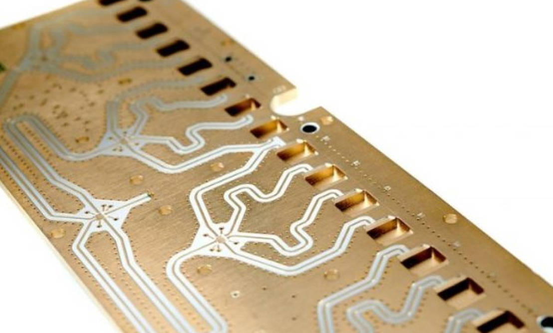
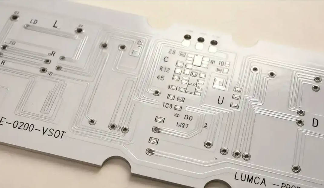
A 3D PCB, more accurately known as a 3D-Molded Interconnect Device (3D-MID), represents a paradigm shift from flat, planar circuitry. Instead of mounting components onto a flat board, 3D-MID technology integrates the electrical circuit directly onto the surface of a three-dimensional, injection-molded plastic part. This transforms the very housing or structural component of a product into its own circuit board, eliminating the need for a separate PCB and connecting cables. It’s a technology that truly merges the electrical and mechanical worlds.
Beyond Flatland: The Concept of 3D-Molded Interconnect Devices (3D-MID)
The philosophy behind 3D-MID is to use space as efficiently as possible. In products with complex shapes and severe space constraints, a flat PCB can be a major design obstacle. A 3D-MID overcomes this by allowing circuit traces to follow the curves and contours of the product’s body. Imagine an antenna integrated directly into the curved casing of a smart device, or a sensor’s circuitry printed onto the very surface of the sensor housing itself. This level of integration leads to significant miniaturization, weight reduction, and the potential for entirely new product form factors that were previously impossible.
How are 3D PCBs Made? Laser Direct Structuring (LDS) and Other Methods
The most prominent manufacturing process for 3D-MIDs is Laser Direct Structuring (LDS). This innovative process involves two main steps. First, the component is injection-molded using a special thermoplastic doped with a laser-activatable metal-organic additive. Second, a laser beam is precisely directed across the surface of the plastic part, tracing the path where the circuit should be. The laser’s energy activates the metal additive in the plastic, creating a microrough surface that is receptive to metallization. The part is then submerged in an electroless copper bath, where copper adheres *only* to the laser-activated paths, forming the conductive circuit traces. Other methods like two-shot molding exist, but LDS offers superior flexibility for intricate patterns.
Key Advantages and Ideal Use Cases
The main benefit of 3D-MID technology is its unparalleled spatial efficiency and design freedom. By turning a mechanical part into an electrical one, it reduces the total number of components, assembly steps, and potential points of failure (like connectors and cables). This results in smaller, lighter, and often more reliable products. The ideal use cases for 3D PCBs are where these benefits are paramount:
- Wearable Technology: Smartwatches, fitness trackers, and hearables where every millimeter counts.
- Medical Devices: Hearing aids, surgical tools, and implantable sensors that must conform to anatomical shapes.
- Automotive Sensors: Steering wheel controls, camera modules, and pressure sensors integrated into complex housings.
- IoT Devices: Compact sensors and smart home components with unique form factors.
Head-to-Head Comparison: Multilayer PCB vs. 3D PCB
To truly understand which technology fits your project, a direct comparison across key attributes is essential. While both serve to connect electronic components, their approaches, strengths, and limitations are fundamentally different.
| Feature | Multilayer PCB | 3D PCB (3D-MID) |
|---|---|---|
| Form Factor | Planar (2D). Limited to flat surfaces, though can be incorporated into rigid-flex designs. | Three-dimensional. Circuits conform to the shape of the component. |
| Spatial Efficiency | Efficient in the Z-axis (stacking layers) but requires a dedicated flat area within the product. | Extremely high. Uses the product’s housing as the circuit substrate, maximizing internal volume. |
| Component Density | Very high. Can support thousands of components and fine-pitch packages like BGAs. | Lower. Generally suited for less dense circuits; placing complex, high-pin-count components can be challenging. |
| Manufacturing Process | Mature and widely available subtractive process (lamination, etching, drilling). | Additive process (e.g., Laser Direct Structuring) requiring specialized materials and equipment. |
| Prototyping & Iteration | Relatively fast and inexpensive for prototypes. Standardized processes allow for quick turns. | Slower and more expensive. Changes often require new injection molding tools, which is a significant cost. |
| Cost | Low NRE (Non-Recurring Engineering) costs. Unit price is highly competitive, especially at scale. | High initial tooling cost (injection mold). Unit cost can be competitive at very high volumes by reducing assembly labor. |
| Best For | Complex, high-performance electronics in conventional form factors (e.g., motherboards, phones). | Miniaturized products with unconventional shapes where space and integration are the highest priorities. |
How to Decide? Key Factors for Your Product’s Success
The choice between these two powerful technologies is not about which one is superior overall, but which is the optimal solution for your specific application. Answering a few key questions about your product’s requirements will illuminate the correct path forward.
When Should You Choose a Multilayer PCB?
A multilayer PCB remains the default and most practical choice for the vast majority of electronic products. Opt for a multilayer PCB when your project aligns with these criteria:
- High Circuit Complexity: If your design involves microprocessors, FPGAs, large memory arrays, or high-speed data buses, the structured layering and controlled impedance of a multilayer board are essential for performance and reliability.
- Standard Form Factor: If your product has a relatively conventional shape (rectangular, square, circular) and can accommodate a flat circuit board, there is no need to add the complexity and cost of a 3D solution.
- Cost-Sensitivity at Low-to-Medium Volumes: The mature manufacturing ecosystem for multilayer PCBs makes them highly cost-effective from prototyping through to mass production. The upfront NRE costs are significantly lower than the tooling required for 3D-MIDs.
- Need for Rapid Iteration: The design-to-prototype cycle for multilayer PCBs is fast and affordable, allowing your team to test, validate, and revise designs quickly without incurring massive tooling costs for each iteration.
When is a 3D PCB the Right Choice?
A 3D PCB is a specialized solution that provides a powerful competitive advantage in the right context. Consider a 3D PCB (3D-MID) when your product’s success hinges on these factors:
- Extreme Miniaturization and Space Constraints: When you are designing a product like a hearing aid or an IoT sensor where every cubic millimeter is critical, integrating circuitry onto the housing is a game-changer. It eliminates the volume that a separate PCB and its connectors would occupy.
- Unconventional or Ergonomic Form Factor: For products that must be curved, ergonomic, or otherwise non-planar, 3D-MID allows the electronics to follow the product’s shape seamlessly. This is a key enabler for wearables and medical implants.
- Simplification and Reliability: If your current design uses a complex assembly of a small PCB, flex circuits, and connectors to fit into a tight space, a 3D-MID can replace that entire assembly with a single, integrated part. This reduces assembly steps, labor costs, and potential points of failure, increasing overall product reliability.
- High-Volume Production: While the initial tooling cost is high, the per-unit cost of 3D-MIDs can become very competitive at high manufacturing volumes (typically hundreds of thousands of units) due to the highly automated process and reduced manual assembly.
The Future of Circuit Design: Are 3D PCBs the Next Big Thing?
While multilayer PCBs will continue to be the workhorse of the electronics industry for the foreseeable future, 3D-MID technology is not just a niche player; it’s a window into the future of product design. The trend across all sectors is toward more integrated, intelligent, and compact devices. 3D PCBs directly serve this trend by breaking down the traditional barrier between the mechanical structure and the electronic function of a product. As manufacturing techniques like LDS become more refined and accessible, and as new materials are developed, we can expect to see wider adoption of this technology.
The future likely lies not in a complete replacement of one technology by the other, but in a hybrid approach. We may see products that use a dense, high-performance multilayer PCB for the core “brain” of the device, connected to multiple 3D-MID components that act as smart peripherals, sensors, or antennas. This combination would leverage the strengths of both worlds: the raw processing power enabled by multilayer density and the ultimate spatial integration offered by 3D circuitry. This collaborative evolution will enable the next generation of truly seamless and intelligent products.
Conclusion: Making the Right Choice for Innovation and Functionality
The decision between a multilayer PCB and a 3D PCB is a strategic one that directly impacts your product’s form, function, cost, and manufacturability. There is no single “best” option—only the right fit for your specific goals. Multilayer PCBs offer a mature, cost-effective, and powerful solution for handling complex electronics within conventional planar constraints. They are the proven foundation of modern technology. 3D PCBs, or 3D-MIDs, offer a revolutionary path forward for products where form factor, miniaturization, and integration are the driving forces of innovation. By carefully evaluating your product’s mechanical constraints, electronic complexity, production volume, and budget, you can confidently select the technology that will not only bring your design to life but also give it a decisive edge in the market.
Multilayer PCB vs 3D PCB, 3D-Molded Interconnect Devices, 3D-MID, PCB technology, choosing the right PCB, Laser Direct Structuring, what is a 3D PCB, electronics design, PCB comparison