Choosing the correct FR4 PCB thickness is a foundational design decision that extends far beyond simple dimensions, critically influencing a circuit’s electrical performance, mechanical robustness, thermal management, and overall manufacturing cost. While 1.6mm (0.062 inches) is the industry-standard thickness, understanding why it’s the standard and when to deviate from it is crucial for optimizing your electronic design for its specific application. This guide provides an in-depth exploration of how board thickness impacts every facet of your project, from signal integrity to final product reliability.
Table of Contents
- What Exactly is FR4 PCB Thickness?
- Standard vs. Custom: A Spectrum of FR4 Thicknesses
- How Does FR4 Thickness Critically Affect Your PCB Design?
- A Practical Guide: How to Choose the Right FR4 Thickness
- Common Pitfalls to Avoid When Specifying PCB Thickness
- Conclusion: Thickness is More Than Just a Number
What Exactly is FR4 PCB Thickness?
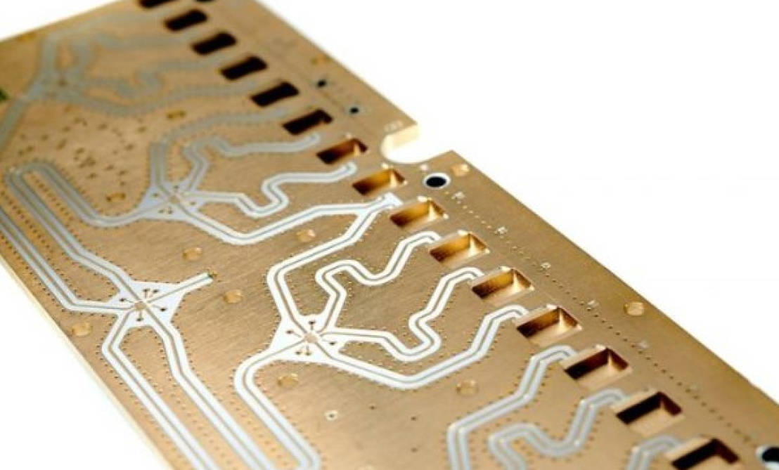
Before diving into the design implications, it’s essential to understand what “PCB thickness” actually refers to. It’s not just a single slab of material. A Printed Circuit Board, especially a multi-layer one, is a composite structure. The total thickness is the cumulative sum of its constituent layers, including the insulating substrate and the conductive copper layers.
Deconstructing the Layers: Core, Prepreg, and Copper Foil
A typical multi-layer PCB is constructed from a combination of a core and prepreg layers. The core is a rigid piece of FR4 laminate that is pre-manufactured with copper foil bonded to both sides. It forms the central, stable part of the board. Prepreg (pre-impregnated) is a sheet of fiberglass cloth impregnated with epoxy resin that is not yet fully cured. These prepreg sheets are used to bond the core(s) and additional copper foil layers together under heat and pressure. The final thickness of your board is the sum of the core thickness, all the prepreg layers, and the copper foil on the outer layers.
Why FR4 is the Industry Standard Material
FR4 is the most common material used for PCBs for several compelling reasons. The name itself is a grade designation: ‘FR’ stands for Flame Retardant, and the ‘4’ indicates it’s a woven glass-reinforced epoxy laminate. It offers an excellent balance of properties that make it suitable for a vast range of applications:
- Cost-Effectiveness: It provides great performance for its price, making it economically viable for mass production.
- Good Electrical Insulation: It has a high dielectric strength, preventing shorts between layers.
- Dimensional Stability: It holds its shape and size well across a range of temperatures and humidity levels.

Standard vs. Custom: A Spectrum of FR4 Thicknesses
While PCBs can be fabricated to nearly any custom thickness, manufacturers have standardized around a set of common dimensions to streamline production and reduce costs. Adhering to these standards whenever possible is a key principle of Design for Manufacturability (DFM).
The Ubiquitous 1.6mm (0.062″): Why is it the Standard?
The 1.6mm (or 1/16th of an inch) standard is not arbitrary. Its prevalence is rooted in historical context and a practical balance of properties. Originally, this thickness was compatible with the card-edge connectors used in early computer systems like the ISA bus. This legacy has persisted because 1.6mm offers an excellent compromise: it is rigid enough for most applications, compatible with a wide array of through-hole components, and is the most cost-effective option due to the high availability of raw materials in this size.
Common FR4 PCB Thickness Options (Table)
Beyond the 1.6mm standard, manufacturers readily offer a range of other thicknesses. Choosing one of these common options is far more economical than specifying a fully custom thickness.
| Thickness (mm) | Thickness (inches) | Typical Applications & Characteristics |
|---|---|---|
| 0.4mm / 0.6mm | 0.016″ / 0.024″ | Ultra-thin. Used in wearables, compact IoT devices, and flexible-rigid sections. Requires careful handling. |
| 0.8mm / 1.0mm | 0.031″ / 0.039″ | Thin. Good for space-constrained designs like USB drives or daughterboards. Offers some flexibility. |
| 1.2mm | 0.047″ | A slightly thinner alternative to the standard, offering minor weight and space savings. |
| 1.6mm | 0.062″ | The Industry Standard. Best balance of cost, rigidity, and component compatibility for general-purpose electronics. |
| 2.0mm / 2.4mm | 0.079″ / 0.094″ | Thick. Used for high-power applications, large boards, or designs requiring extreme rigidity to prevent bending. |
| 3.2mm | 0.125″ | Very Thick. Reserved for mechanically demanding applications like industrial control panels or large power conversion systems. |
How Does FR4 Thickness Critically Affect Your PCB Design?
The choice of board thickness is a pivotal engineering decision with a ripple effect across the entire design. Here’s a breakdown of the key areas it impacts.
Impedance Control and Signal Integrity
For high-speed digital circuits (e.g., USB, HDMI, DDR memory), maintaining a specific characteristic impedance—typically 50 ohms for single-ended traces or 90-100 ohms for differential pairs—is non-negotiable. The thickness of the dielectric material (the FR4 between a signal trace and its reference plane) is a primary variable in the impedance calculation.
- A thicker dielectric layer requires a wider trace to achieve the same impedance. This can consume valuable routing space, especially on dense boards.
- A thinner dielectric layer allows for narrower traces, improving routing density. However, it also brings traces closer to their reference plane and other traces, which can increase parasitic capacitance and the risk of crosstalk between adjacent signals.
Mechanical Strength and Rigidity
The mechanical stability of your PCB is directly proportional to its thickness. A thicker board provides superior rigidity, making it resistant to flexing and vibration. This is crucial for large circuit boards, products subjected to mechanical stress, or designs that support heavy components like transformers, large electrolytic capacitors, or robust connectors. Conversely, thinner boards are more susceptible to warping, especially during the high temperatures of reflow soldering, and can suffer from pad cratering or component failure under physical strain.
Component Compatibility and Placement
Your choice of components can dictate a required thickness. Many through-hole components, such as headers, connectors, and power jacks, are designed with pin lengths optimized for the standard 1.6mm thickness. Using a significantly thicker board may result in pins that are too short to be soldered reliably. Using a much thinner board can lead to excessive pin protrusion, which might interfere with the enclosure or other components. Furthermore, for large Ball Grid Array (BGA) components, a thicker, more stable board is often preferred to minimize flexion that could stress and break solder joints.
Current Carrying Capacity and Thermal Management
While the current-carrying capacity of a trace is primarily determined by its width and copper weight (e.g., 1oz or 2oz), the overall board thickness plays a supporting role in thermal management. A thicker board has a larger thermal mass, allowing it to absorb and spread heat more effectively from high-power components. In high-current applications, thicker boards often incorporate thicker copper weights, and the added rigidity helps manage the physical mass of large power planes and components.
Weight, Size, and Form Factor
In modern electronics, especially portable and wearable devices, every gram and millimeter counts. Using a thinner PCB (e.g., 0.8mm or 0.6mm) can lead to significant reductions in both weight and overall product thickness. This is a critical consideration for devices like smartphones, drones, and medical sensors. Conversely, for stationary industrial equipment, the added weight and bulk of a thicker board are often negligible and are a worthy trade-off for increased durability.
A Practical Guide: How to Choose the Right FR4 Thickness
Navigating these trade-offs requires a systematic approach. Follow these steps to make an informed decision for your project.
Step 1: Define Your Application’s Core Requirements
Start by asking fundamental questions about your project’s purpose and environment.
- High-Speed Digital? If your design includes interfaces like DDR, PCIe, or Ethernet, impedance control is paramount. Your required trace widths may push you toward a specific dielectric thickness, influencing the overall board thickness.
- High-Power? If you are designing a power supply or motor controller, mechanical strength to support heavy components and thermal dissipation will be key. A thicker board (e.g., 2.0mm) is often a safer choice.
- Space-Constrained? For wearables or IoT devices, a thin board (e.g., 0.8mm) is likely necessary to meet form factor requirements.
- Rule of Thumb: Start with the default of 1.6mm. Only deviate if your application presents a specific, compelling reason to do so. This will always be the most cost-effective and readily available option.
Step 2: Considering Copper Weight in Conjunction with Thickness
Board thickness and copper weight are two separate but related specifications. Copper weight is measured in ounces per square foot (oz/ft²). Standard copper is 1oz (35µm thick), but for high-current applications, 2oz, 3oz, or even heavier copper is used. A design that requires heavy copper often benefits from a thicker overall board to provide the necessary mechanical support and layer separation.
Step 3: Consult Your Manufacturer (The DFM Check)
Before finalizing your design, always consult your chosen PCB fabricator. They can provide a list of their standard stackups and thicknesses. Deviating from their standard offerings will almost certainly increase both the cost and the lead time of your project. They can also advise on the manufacturing limitations related to your chosen thickness, such as the minimum trace and space they can achieve or constraints on processes like V-scoring for thinner boards.
Common Pitfalls to Avoid When Specifying PCB Thickness
- Ignoring V-Scoring Limitations: V-scoring, a method for panelizing boards, can be problematic on very thin PCBs (typically <0.8mm) as it can weaken the board excessively.
- Forgetting Component Lead Length: Double-check that your through-hole components will fit properly on a non-standard board thickness.
- Over-Engineering for Simple Designs: Don’t specify a 2.4mm thick board for a simple microcontroller circuit just “to be safe.” This adds unnecessary cost and weight. Stick to 1.6mm unless a clear technical reason exists.
- Neglecting Impedance Calculations: For any design with signals faster than a few hundred MHz, failing to account for how dielectric thickness impacts impedance is a recipe for signal integrity failures.
Conclusion: Thickness is More Than Just a Number
FR4 PCB thickness is a fundamental design parameter, not an afterthought. It is a critical variable in an engineering equation that balances electrical performance, mechanical integrity, manufacturability, and cost. While the 1.6mm standard serves as an excellent and reliable starting point for a majority of projects, a deep understanding of the trade-offs involved allows you to make a deliberate choice that optimizes your design for its intended purpose. By carefully considering the demands of your application—from high-speed signals to mechanical stress—you can select a thickness that ensures your final product is both functional and robust.
FR4 PCB Thickness, standard PCB thickness, PCB design, impedance control, FR4 material, pcb board thickness, how to choose pcb thickness, pcb manufacturing, signal integrity