In high-speed PCB design, crosstalk and reflection are two critical signal integrity issues that can degrade performance and cause system failure. Reflection is an energy “echo” caused by impedance mismatches along a signal’s path, resulting in ringing and distortion of the waveform. Crosstalk, on the other hand, is the unwanted electromagnetic interference between adjacent traces, where a switching signal (the aggressor) induces noise onto a nearby quiet signal (the victim). Understanding the distinct causes and effects of both is fundamental to designing robust and reliable high-speed digital circuits.

Table of Contents
- What is Signal Integrity and Why Does It Matter?
- Understanding Reflection: The “Echo” in Your Traces
- Demystifying Crosstalk: When Signals “Talk” to Each Other
- Crosstalk vs. Reflection: A Head-to-Head Comparison
- A Holistic Approach: Integrating SI Analysis into Your PCB Design Flow
- Conclusion: Designing for Signal Integrity Success
What is Signal Integrity and Why Does It Matter?
As clock speeds and data rates increase, the fundamental principles governing circuit board design shift dramatically. A simple copper trace on a Printed Circuit Board (PCB) no longer behaves like an ideal, zero-resistance wire. Instead, it must be treated as a transmission line, an element with its own characteristic impedance, propagation delay, and susceptibility to electromagnetic fields. Signal Integrity (SI) is the practice of ensuring signals are transmitted from driver to receiver with sufficient quality to be correctly interpreted. Poor signal integrity, caused by issues like reflection and crosstalk, leads directly to tangible problems, including increased bit error rates (BER), system timing violations, intermittent failures, and excessive electromagnetic interference (EMI) that can cause a product to fail compliance testing.
The core challenge arises when the signal’s rise time (the time it takes to transition from low to high) becomes comparable to or shorter than the time it takes for the signal to travel down the trace. At this point, the trace’s physical properties—its width, height above a reference plane, and the dielectric constant of the PCB material—dominate the circuit’s behavior. Neglecting these high-speed effects is a primary cause of project delays and costly board respins. Therefore, a proactive approach to managing signal integrity is not an option but a necessity for modern electronic product design.
Understanding Reflection: The “Echo” in Your Traces
Signal reflection is a phenomenon where a portion of the signal’s energy is reflected back toward the source when it encounters a change in impedance along its path. Imagine speaking into a long canyon; your voice travels, hits the far wall, and an echo travels back. Similarly, when a high-speed electrical signal traveling down a trace of a certain characteristic impedance (Z₀) encounters a different impedance—at a connector, a component pin, or a via—a part of its energy bounces back. This reflected energy combines with the original signal, causing distortions such as overshoot (voltage exceeding the intended high level), undershoot (voltage dropping below the intended low level), and ringing (oscillations that settle over time). These distortions can lead to false logic switching, damage to input protection diodes, and degraded timing margins.
What Causes Signal Reflection?
The root cause of reflection is impedance mismatch. Every transmission line on a PCB has a characteristic impedance (Z₀), typically designed to be 50 ohms for single-ended signals. Reflection occurs when the signal path impedance (Z) deviates from the source (driver) or load (receiver) impedance. The amount of reflection is quantified by the reflection coefficient (Γ), calculated as Γ = (Z_L – Z₀) / (Z_L + Z₀), where Z_L is the load impedance. A perfect match (Z_L = Z₀) results in a reflection coefficient of zero, meaning all energy is absorbed by the load. Common sources of impedance discontinuities include:
- Unterminated Traces: Leaving a trace end “open” creates a massive impedance mismatch, causing significant reflections.
- Vias: A via introduces both capacitive and inductive discontinuities, altering the local impedance.
- Connectors and Sockets: These components have their own impedance characteristics that may not match the PCB traces.
- Trace Stubs: Unused branches on a signal trace act as antennas and create severe impedance mismatches.
- Changes in Trace Geometry: Variations in trace width or changing reference planes without proper care will alter the characteristic impedance.
How to Identify Reflection on a PCB
Identifying reflection can be done through both measurement and simulation. The most direct method is using a high-bandwidth oscilloscope to probe a signal line. The classic signs of reflection—overshoot, undershoot, and ringing—will be clearly visible on the signal’s rising and falling edges. For more in-depth analysis, a Time-Domain Reflectometer (TDR) is an invaluable tool. A TDR sends a fast-step pulse down the trace and measures the reflections over time. This allows engineers to not only detect the presence of reflections but also to physically locate the exact position of the impedance mismatch on the board, whether it’s a poorly designed via, a connector, or a sharp bend.
Beyond physical measurement, modern EDA (Electronic Design Automation) tools offer powerful pre-layout and post-layout simulation capabilities. By creating accurate models of your PCB stack-up, traces, and components, you can simulate signal behavior before a single piece of copper is etched. These simulations can predict reflection issues with high accuracy, allowing you to iterate and optimize your design virtually, saving immense time and cost associated with physical prototypes and debugging.
Proven Strategies to Mitigate Reflection
Mitigating reflection is primarily about maintaining a constant impedance from the driver to the receiver. This is achieved through two main strategies: controlled impedance routing and proper termination.
- Controlled Impedance Routing: This is the foundation of high-speed design. It involves carefully calculating the trace width, its height above the reference ground/power plane, and selecting a PCB material with a known dielectric constant (Er) to achieve a target characteristic impedance (e.g., 50Ω).
- Proper Termination Schemes: Termination involves adding resistors to the circuit to match the trace impedance, thereby absorbing the signal energy and preventing reflections. The choice of termination depends on the application, power consumption, and topology.
| Termination Scheme | Description | Pros | Cons |
|---|---|---|---|
| Series Termination | A resistor is placed in series with the driver, close to the source. The resistor value plus the driver’s output impedance should equal the trace’s characteristic impedance. | Low power consumption; single component. | Degrades signal rise time; only effective for point-to-point topologies. |
| Parallel Termination | A resistor is placed at the receiver end, connected between the signal line and ground (or VCC). The resistor value should match the trace impedance. | Excellent signal quality; works for multiple loads. | High static power consumption when the signal is high (if terminated to GND). |
| Thevenin Termination | A voltage divider (two resistors, one to VCC and one to GND) is placed at the receiver. The parallel equivalent resistance should match the trace impedance. | Provides a solid DC bias level; good signal integrity. | Highest static power consumption; requires two components. |
| AC Termination | A resistor and capacitor are placed in series at the receiver end, connected to ground. | No static power consumption. | Adds delay; capacitor value needs careful selection. |
In addition to termination, good routing hygiene is crucial. Always use 45-degree bends instead of sharp 90-degree corners, as right-angle bends create a local impedance discontinuity. Eliminate any unnecessary trace stubs and ensure a solid, uninterrupted reference plane runs directly beneath your high-speed traces.
Demystifying Crosstalk: When Signals “Talk” to Each Other
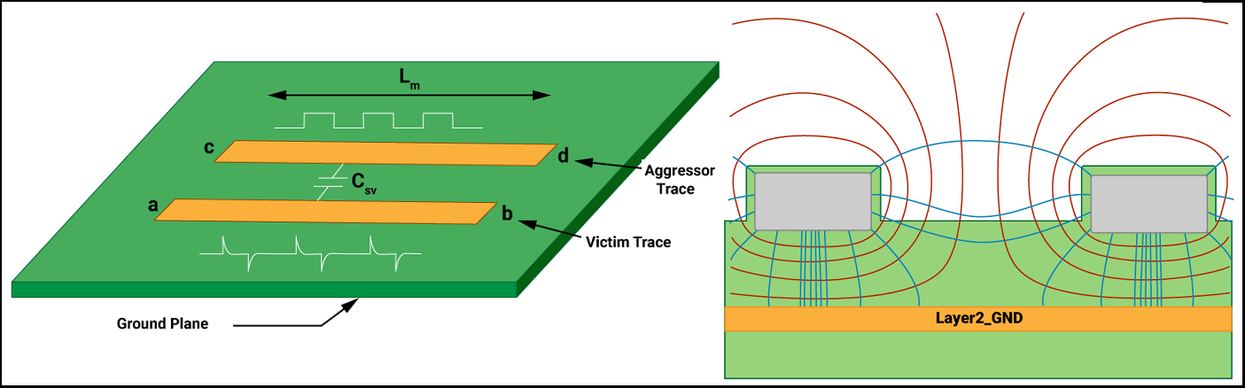
Crosstalk, also known as cross-coupling, is the unintentional transfer of energy between adjacent signal traces on a PCB. In this scenario, a signal trace with a switching voltage or current is called the aggressor, while the nearby trace that picks up the unwanted noise is the victim. This is analogous to hearing a faint, adjacent conversation on an old analog phone line. In a digital circuit, this injected noise can reduce noise margins, cause false logic transitions, and introduce timing jitter. As signal speeds and board densities increase, traces are packed closer together, making crosstalk a more prominent and challenging signal integrity issue.
What is the Root Cause of Crosstalk?
Crosstalk is fundamentally caused by the electromagnetic fields that surround a current-carrying trace. These fields can couple to adjacent traces in two primary ways:
- Capacitive (Electric Field) Coupling: This occurs due to the parasitic capacitance between two parallel traces. As the voltage on the aggressor trace changes (dV/dt), it induces a current in the victim trace through this mutual capacitance. Capacitive coupling is strongest when traces are close together over a long distance and is proportional to the rate of voltage change (the signal’s slew rate).
- Inductive (Magnetic Field) Coupling: This occurs due to the magnetic field generated by the changing current (dI/dt) in the aggressor trace’s loop area (the area formed by the signal trace and its return path). This changing magnetic field induces a voltage in the parallel victim trace’s loop area. Inductive coupling is stronger when the traces are closer to each other and farther from their reference ground plane.
This coupling results in two types of crosstalk noise on the victim line: Near-End Crosstalk (NEXT), which is the noise pulse that travels back toward the driver on the victim line, and Far-End Crosstalk (FEXT), which is the noise pulse that travels forward in the same direction as the aggressor signal.
How Can You Detect Crosstalk?
Detecting crosstalk involves correlating noise on a victim line with activity on a potential aggressor. Using an oscilloscope, you can trigger on the rising or falling edge of a suspected aggressor signal and observe the victim line for corresponding noise glitches. If a quiet line, held at a steady logic high or low, shows noise spikes that align perfectly with the switching of a neighboring signal, you have found crosstalk. A powerful visualization tool for assessing the combined impact of crosstalk, reflection, and other noise sources is the Eye Diagram. By overlaying many signal transitions, an eye diagram shows the effective signal integrity; crosstalk will cause the eye to “close” vertically, reducing the noise margin.
Similar to reflection analysis, SI simulation tools are the most effective way to proactively identify and quantify crosstalk. Engineers can set up simulations to target specific nets, and the software will calculate the level of NEXT and FEXT based on the board layout, stack-up, and driver models. This allows for what-if analysis, such as “How much does the crosstalk reduce if I increase the spacing from 4 mils to 8 mils?”
Effective Techniques for Crosstalk Mitigation
Since crosstalk is caused by electromagnetic coupling, mitigation techniques focus on reducing that coupling by controlling trace geometry and providing adequate shielding.
- Increase Trace Spacing: This is the single most effective way to reduce crosstalk. The coupling fields decay rapidly with distance. A common guideline is the 3W Rule, which states that the spacing between traces should be at least three times the width of a single trace. For critical signals, a spacing of 5W or even 10W may be necessary.
- Utilize Ground Planes: Routing high-speed traces on a layer adjacent to a solid ground plane is crucial. This creates a tight current return path, minimizing the loop area and thus reducing inductive coupling. Routing traces between two ground planes (a stripline configuration) provides even better shielding and virtually eliminates far-end crosstalk.
- Route Orthogonally: On adjacent signal layers, route traces perpendicularly (e.g., horizontal on one layer, vertical on the next). This minimizes the parallel run length between traces on different layers, significantly reducing broadside coupling.
- Use Guard Traces: A guard trace is a grounded trace routed parallel to a sensitive signal. It can help “absorb” the coupling fields from an aggressor, but it must be frequently connected to the main ground plane with stitching vias to be effective.
- Embrace Differential Signaling: For very high-speed interfaces (like USB, Ethernet, PCIe), differential pairs are used. Because the two signals are equal and opposite, their electromagnetic fields largely cancel each other out, making them highly immune to crosstalk and other noise sources.
Crosstalk vs. Reflection: A Head-to-Head Comparison
While both are critical SI issues, it’s important to remember their distinct nature. Fixing a reflection problem with a crosstalk solution will not work. The following table provides a clear summary of their differences.
| Attribute | Signal Reflection | Crosstalk |
|---|---|---|
| Core Phenomenon | Energy “echo” on the same trace. | Energy “bleeding” between adjacent traces. |
| Primary Cause | Impedance mismatch (discontinuity). | Electromagnetic (capacitive & inductive) coupling. |
| Visual Effect on Signal | Overshoot, undershoot, ringing, stair-stepping. | Noise glitches and pulses on a quiet victim line. |
| Primary Mitigation Strategy | Impedance Control & Termination. Maintain a consistent impedance path and use termination resistors. | Spacing & Shielding. Increase distance between traces and use reference planes effectively. |
| Key Design Rule | Match trace impedance to source/load impedance. | Follow spacing rules like the 3W rule. |
A Holistic Approach: Integrating SI Analysis into Your PCB Design Flow
The most successful engineering teams treat signal integrity not as a final-stage debugging problem but as an integral part of the entire design process. A modern, holistic approach involves a “correct-by-construction” methodology, where SI principles guide design choices from the very beginning. This starts with a robust pre-layout simulation phase, where you define the PCB stack-up, select materials, and simulate critical traces to determine the required impedance profiles and termination strategies.
Once the initial design rules are established, they should be entered as constraints into your primary EDA tool (e.g., Altium Designer, Cadence Allegro, Siemens Xpedition). These tools can then enforce rules during layout, such as minimum trace spacing, matched length for differential pairs, and maximum stub lengths. This automated checking prevents many common SI errors. Finally, after routing is complete, a post-layout verification simulation should be run using the actual, extracted trace geometries. This final check confirms that the design meets all timing and noise margin requirements before committing to fabrication, creating a powerful feedback loop for continuous improvement and first-pass success.
Conclusion: Designing for Signal Integrity Success
Crosstalk and reflection are predictable consequences of physics in high-speed digital systems. They are not random, mysterious gremlins but manageable challenges that can be overcome with knowledge and proper design discipline. Reflection is an intra-trace issue solved with impedance control and termination, while crosstalk is an inter-trace issue solved with spacing and shielding. By understanding their distinct causes, learning how to identify their signatures, and applying the proven mitigation techniques discussed, you can move from a reactive debugging cycle to a proactive design methodology.
Ultimately, a deep understanding of signal integrity empowers you to design faster, denser, and more reliable electronic products. Investing time in pre-layout analysis, adhering to strict layout rules, and leveraging the power of modern simulation tools will always be more cost-effective than troubleshooting a failing prototype on the lab bench. By treating every high-speed trace as a transmission line, you pave the way for signal integrity success.