Choosing the optimal PCB layer count—be it 4-layer, 6-layer, or 8-layer—is a critical decision in electronics design, profoundly impacting a product’s performance, cost, and manufacturability. The ideal choice hinges on a careful evaluation of design complexity, signal speed, power delivery requirements, EMI concerns, and budget constraints. While a 4-layer PCB offers a cost-effective solution for simpler designs, 6-layer and 8-layer PCBs provide superior signal integrity, improved EMI suppression, and greater routing density, essential for high-speed, complex, or densely packed electronic systems.
Understanding Multi-Layer PCBs: An Overview of Stackup Benefits
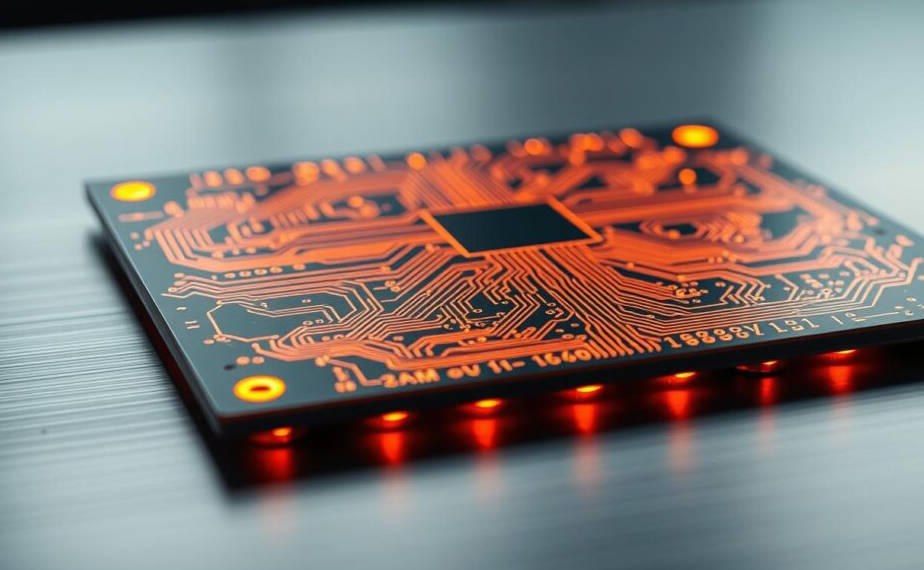
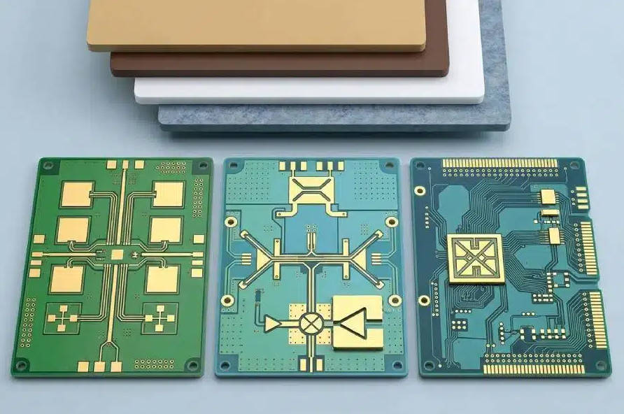
Multi-layer Printed Circuit Boards (PCBs) are foundational to modern electronics, providing a compact and efficient platform for complex circuitry. Unlike single or double-sided boards, multi-layer PCBs integrate multiple conductive layers, separated by insulating dielectric materials and bonded together under high pressure and temperature. This layered construction offers significant advantages, including increased routing density, reduced board size, enhanced electrical performance, and improved electromagnetic compatibility (EMC).
The primary benefit of moving from a simple 2-layer board to a 4, 6, or 8-layer stackup is the ability to dedicate internal layers to specific functions, such as ground planes and power planes. These dedicated planes act as stable references for signals, provide low-impedance paths for current return, and significantly improve power delivery network (PDN) performance. Furthermore, internal layers can be used for shielding sensitive signals, isolating noisy traces, and managing thermal dissipation more effectively. This strategic distribution of functionality across layers is what ultimately defines the capabilities and performance characteristics of a multi-layer PCB.
What are the fundamental advantages of increasing PCB layer count?
Increasing the number of layers in a PCB directly translates to several fundamental advantages critical for advanced electronic designs. Firstly, it dramatically enhances routing density. With more layers available, designers can route more traces in a smaller area, enabling highly compact and miniature electronic devices. This is particularly crucial for portable electronics, wearables, and embedded systems where space is at a premium.
Secondly, higher layer counts significantly improve signal integrity (SI). Dedicated ground and power planes provide excellent return paths for high-speed signals, minimizing loop inductance and preventing signal degradation from reflections, crosstalk, and impedance mismatches. This results in cleaner signals, faster data rates, and more reliable operation, especially in applications involving high-frequency components or communication protocols like PCIe, DDR, or Ethernet.
Thirdly, multi-layer boards offer superior electromagnetic interference (EMI) suppression. Ground and power planes act as effective shields, containing electromagnetic fields within the board and preventing them from radiating outwards or coupling into adjacent traces. This is vital for meeting regulatory compliance standards (e.g., FCC, CE) and ensuring the reliable operation of sensitive circuits in noisy environments. Finally, a well-designed multi-layer stackup facilitates better power delivery by providing low-impedance power distribution networks (PDN), ensuring stable voltage supplies to all components, even under dynamic load conditions.
4-Layer PCB: The Cost-Effective Workhorse
The 4-layer PCB represents a common entry point into multi-layer design, offering a significant upgrade from double-sided boards without incurring excessive costs. Its typical stackup involves two outer signal layers and two internal layers, often configured as a dedicated ground plane and a dedicated power plane (e.g., Signal-Ground-Power-Signal). This configuration strikes a balance between cost, manufacturability, and performance, making it suitable for a wide range of applications.
The primary appeal of a 4-layer board lies in its economic efficiency. Manufacturing costs are relatively low compared to higher layer counts, and fabrication processes are well-established and widely available. This makes it an attractive option for projects with tight budgets or those requiring high-volume production where cost-per-unit is a critical factor. Despite its simplicity, a properly designed 4-layer board can effectively manage moderately high-speed signals and address basic EMI concerns, provided the layout rules are strictly followed.
When to choose a 4-layer PCB: Applications and limitations
A 4-layer PCB is an excellent choice for a variety of applications that do not demand extreme performance or very high component density. These include general-purpose microcontrollers, simple embedded systems, IoT devices, audio circuits, low-frequency communication boards, and power supply units. It’s particularly suitable when the design has a moderate number of components, signal speeds are below ~100 MHz, and electromagnetic compatibility requirements are not exceptionally stringent.
However, 4-layer PCBs do come with limitations. The availability of only two signal layers can lead to routing congestion, especially with higher pin-count components or complex interconnections. The single ground plane and single power plane, while effective, might not offer optimal isolation for all high-speed signals or adequately manage complex power delivery networks required by modern FPGAs or high-performance processors. Consequently, achieving pristine signal integrity and robust EMI suppression for very high-speed designs can be challenging, often requiring more elaborate layout techniques or compromises in routing. For instance, creating effective microstrip or stripline structures for controlled impedance can be more restrictive.
6-Layer PCB: Balancing Performance and Cost
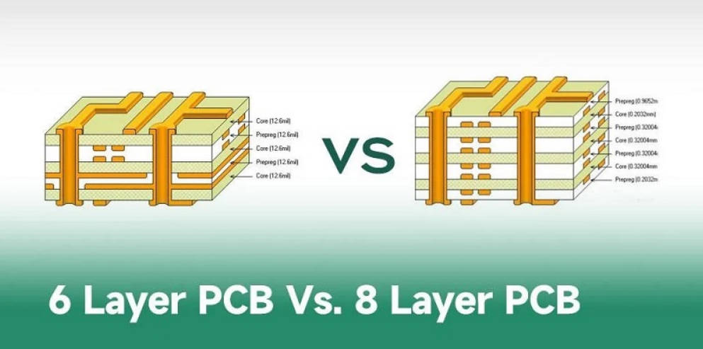
The 6-layer PCB is often considered the sweet spot for many intermediate to high-performance designs, offering a substantial leap in capabilities over a 4-layer board while remaining more cost-effective than 8-layer or higher solutions. A common 6-layer stackup might look like Signal-Ground-Signal-Signal-Power-Signal or Signal-Ground-Signal-Power-Ground-Signal, providing increased flexibility for routing, improved signal integrity, and enhanced EMI control.
The addition of two extra layers, typically signal and/or ground planes, allows for more sophisticated design strategies. Designers can dedicate more layers to high-speed signals, provide multiple ground references, or create a more robust power distribution network. This increased real estate and structural flexibility directly translates to better electrical performance, making the 6-layer PCB a popular choice for a broader range of complex applications.
Advantages of a 6-layer stackup over 4-layer for high-speed design
For high-speed designs, the advantages of a 6-layer stackup over a 4-layer are pronounced. One key benefit is the ability to create multiple dedicated signal layers that are adjacent to continuous ground planes. For example, a stackup like Signal-Ground-Signal-Signal-Power-Signal allows for two internal signal layers to be directly referenced to a ground plane, forming effective stripline or microstrip transmission lines with controlled impedance. This is crucial for minimizing reflections and crosstalk for signals operating at hundreds of megahertz or even gigahertz speeds.
Furthermore, the extra layers provide greater flexibility in separating noisy digital signals from sensitive analog signals, thus reducing mutual interference. Designers can strategically place high-speed traces on internal layers, sandwiched between ground planes, effectively shielding them from external radiation and vice-versa. The additional ground/power planes also lead to a lower impedance PDN, crucial for maintaining stable voltage levels for power-hungry digital components. This improved power integrity directly supports the reliable operation of high-speed ICs and reduces overall system noise, making the 6-layer PCB a more robust solution for demanding applications such as computing peripherals, advanced networking equipment, and complex industrial control systems.
8-Layer PCB: Maximizing Performance and Density
The 8-layer PCB represents a significant commitment to maximizing performance, signal integrity, and routing density. With eight conductive layers, designers gain unparalleled flexibility in creating highly optimized stackups that cater to the most demanding electronic applications. Common 8-layer configurations include variations like Signal-Ground-Signal-Power-Power-Signal-Ground-Signal or Signal-Ground-Signal-Ground-Signal-Power-Ground-Signal, emphasizing multiple ground and power planes to achieve superior electrical characteristics.
This increased layer count is primarily driven by the need to support extremely high-speed interfaces, highly integrated components (e.g., large FPGAs, ASICs with thousands of pins), and designs requiring stringent control over electromagnetic compatibility. While the manufacturing cost is notably higher, the performance benefits often outweigh the expense for mission-critical or bleeding-edge technologies.
When to opt for an 8-layer PCB: Ultra-high speed and complex designs
An 8-layer PCB becomes essential when dealing with designs characterized by ultra-high-speed signals (e.g., multi-gigabit transceivers, DDR4/DDR5 memory interfaces), very high component density, or extremely low noise requirements. Applications that frequently demand 8-layer or higher PCBs include high-performance servers, advanced telecommunications equipment, complex graphics cards, military/aerospace systems, and sophisticated medical imaging devices. In these scenarios, the ability to dedicate multiple internal layers to provide solid ground and power planes, alongside multiple signal layers, is paramount.
The benefits are manifold: superior signal integrity is achieved through multiple continuous ground references, minimizing return path impedance and crosstalk for critical high-speed traces. EMI suppression reaches its peak, as internal signal layers can be completely buried between ground planes, providing maximum shielding. Power delivery networks become exceptionally robust, capable of handling dynamic current loads with minimal voltage ripple. Furthermore, the sheer number of routing layers allows for the elegant resolution of complex routing challenges, leading to a compact board footprint even with highly integrated components, making an 8-layer PCB the gold standard for state-of-the-art electronic products where compromise on performance is not an option.
Key Decision Factors: How to Choose Your PCB Layer Count
The decision between a 4-layer, 6-layer, or 8-layer PCB is not arbitrary; it’s a strategic engineering choice influenced by several critical factors. Designers must weigh these considerations against their project goals, balancing performance requirements with practical constraints. Understanding the interplay of these factors is crucial for making an informed decision that optimizes both the functionality and cost-effectiveness of the final product.
| Feature/Factor | 4-Layer PCB | 6-Layer PCB | 8-Layer PCB |
|---|---|---|---|
| Cost (Relative) | Low (Most Economical) | Medium | High (Most Expensive) |
| Routing Density | Limited | Moderate to High | Very High (Maximized) |
| Signal Integrity | Good for moderate speeds, careful layout needed | Very Good (Improved return paths, controlled impedance) | Excellent (Multiple dedicated Gnd/Pwr, optimal impedance) |
| EMI/EMC Performance | Basic shielding, careful design required | Good shielding, better noise isolation | Excellent shielding, superior noise suppression |
| Power Delivery Network (PDN) | Adequate for basic needs | Improved stability and lower impedance | Robust and low impedance for high current |
| Design Complexity | Simpler, easier to manage | Moderate, more stackup options | High, requires advanced stackup planning |
| Manufacturing Complexity | Lower, higher yield | Medium | Higher, potentially lower yield |
| Typical Applications | IoT, simple MCUs, low-freq comms, basic power | Advanced MCUs, DDR3/DDR4, PCIe Gen1/2, networking | High-speed FPGAs/ASICs, DDR4/DDR5, PCIe Gen3+, servers, aerospace |
Evaluating Signal Integrity and High-Speed Considerations
For any PCB, signal integrity (SI) is paramount, especially as operating frequencies increase. High-speed signals are susceptible to issues like reflections, crosstalk, ground bounce, and power supply noise, all of which can degrade signal quality and lead to system malfunction. The choice of layer count directly impacts SI because it determines the availability and effectiveness of ground and power planes, which are crucial for providing stable return paths and controlled impedance traces.
With a 4-layer PCB, designers must be diligent about routing high-speed signals, often relying on careful trace length matching and minimizing layer transitions. The single ground plane may lead to longer return paths and increased inductance, making it harder to maintain impedance control for differential pairs. In contrast, 6-layer and 8-layer PCBs offer multiple continuous ground and power planes, allowing for ideal stripline or symmetric stripline configurations. These configurations bury high-speed traces between ground planes, providing consistent impedance and excellent shielding. The ability to create dedicated ground and power reference layers significantly reduces loop inductance, minimizes ground bounce, and enhances overall signal quality, making higher layer counts indispensable for designs involving high-frequency data transmission like gigabit Ethernet, high-speed serial links, or advanced memory interfaces.
Analyzing EMI/EMC Requirements and Shielding Effectiveness
Electromagnetic Interference (EMI) and Electromagnetic Compatibility (EMC) are critical concerns in modern electronics, dictating a product’s ability to operate without causing or succumbing to electromagnetic disturbances. The PCB layer count plays a pivotal role in managing EMI/EMC. Higher layer counts generally offer superior EMI suppression and shielding effectiveness due to the increased presence of solid ground and power planes. These planes act as a Faraday cage, containing electromagnetic fields within the board and preventing them from radiating outwards or coupling into other sensitive circuits.
A 4-layer board, with its limited planes, may struggle to meet stringent EMI requirements, often necessitating additional external shielding or more complex filtering at the system level. High-speed signals on outer layers are more prone to radiating noise. As we move to 6-layer and especially 8-layer PCBs, the ability to sandwich high-speed signal layers between continuous ground planes provides inherent shielding. This ‘burial’ of critical signals significantly reduces their potential for radiation and also protects them from external noise. Furthermore, multiple ground planes offer lower impedance return paths for high-frequency currents, minimizing ground loops and common-mode noise. This intrinsic EMI protection offered by higher layer counts can simplify compliance testing, reduce design iterations, and ultimately lead to a more robust and reliable product in electrically noisy environments.
The Impact of Component Density and Routing Complexity
The sheer number of components and the intricacy of their interconnections are major drivers for increasing PCB layer count. As electronic systems become more integrated and miniaturized, designers face the challenge of routing hundreds or even thousands of connections in a limited space. High pin-count devices like FPGAs, ASICs, and BGA packages demand extensive routing channels, and managing these on fewer layers can quickly lead to an unroutable board or one with significant performance compromises.
A 4-layer PCB offers limited routing real estate, which might be sufficient for simpler designs with few components. However, for boards featuring multiple ICs, complex power schemes, or numerous I/O lines, routing on 4 layers can become an arduous task, often requiring excessive use of vias (which degrade signal integrity) or leading to a larger board size. A 6-layer PCB provides a significant increase in routing capacity, allowing for more efficient trace placement, easier separation of signal types, and better organization of power and ground nets. The jump to an 8-layer PCB further amplifies this, offering maximal routing density. Designers can strategically assign different signal groups to distinct layers, simplify trace fan-out from BGA packages, and create clear, unobstructed signal paths, leading to a more compact and performant design. This increased density not only enables smaller product footprints but also simplifies the layout process for complex designs, reducing design time and potential errors.
Cost Considerations and Manufacturing Feasibility
Cost is undeniably a dominant factor in PCB design, and the number of layers directly correlates with manufacturing expenses. Each additional layer adds to the material cost (more prepreg and core material), fabrication time (more lamination cycles, drilling, plating steps), and complexity of the manufacturing process. Therefore, increasing the layer count without a justifiable technical reason can significantly inflate the product’s bill of materials (BOM) and overall production cost.
A 4-layer PCB is typically the most cost-effective option for multi-layer boards, benefiting from mature manufacturing processes and higher production yields. As the layer count increases to 6, and then to 8, the manufacturing complexity rises. This includes tighter tolerances for drilling and etching, increased risk of delamination during lamination, and more stringent quality control requirements. This translates to higher per-board costs and potentially longer lead times, especially for prototypes or smaller production runs. Designers must perform a thorough cost-benefit analysis, comparing the additional performance gains of a higher layer count against the increased manufacturing cost. Sometimes, a more optimized 4-layer or 6-layer design with careful layout planning can achieve satisfactory performance for less, making it crucial to avoid over-engineering the layer count unless absolutely necessary for performance or density requirements.
Advanced Stackup Strategies and Best Practices
Beyond simply choosing a layer count, the specific arrangement of layers—the PCB stackup—is paramount for achieving optimal performance. An intelligently designed stackup can significantly enhance signal integrity, reduce EMI, and improve power delivery, regardless of the total layer count. Conversely, a poorly designed stackup can negate the benefits of even an 8-layer board.
Key principles include ensuring signal layers are adjacent to solid reference planes (ground or power), providing multiple ground planes for high-speed designs, and symmetrically distributing layers to prevent warp and twist during manufacturing. For example, in high-speed applications, burying critical signals between two ground planes (stripline) offers superior shielding and impedance control compared to placing them on outer layers (microstrip). Similarly, separating power and ground planes with a thin dielectric can create a high-capacitance power distribution network, which helps filter noise and maintain stable voltage rails.
Optimal stackup configurations for 4, 6, and 8 layer PCBs
For a 4-Layer PCB: The most common and effective 4-layer stackup is Signal-Ground-Power-Signal.
- Layer 1 (Top): Signal Layer (components, critical high-speed signals).
- Layer 2 (Internal): Solid Ground Plane (reference for L1, L3 signals, EMI shield).
- Layer 3 (Internal): Solid Power Plane (stable power distribution, return path for L4 signals).
- Layer 4 (Bottom): Signal Layer (less critical signals, routing access).
This stackup provides clear reference planes for both outer signal layers, though the power plane on L3 may not be an ideal return path for all L4 signals. A variation might swap L3 and L4 to keep a solid plane closer to the bottom signal layer, depending on the design needs.
For a 6-Layer PCB: A common high-performance 6-layer stackup is Signal-Ground-Signal-Signal-Power-Signal (or similar).
- Layer 1 (Top): Signal Layer (components, critical signals).
- Layer 2 (Internal): Solid Ground Plane (reference for L1, L3 signals, EMI shield).
- Layer 3 (Internal): Signal Layer (high-speed signals referenced to L2).
- Layer 4 (Internal): Signal Layer (or Ground plane for better stripline).
- Layer 5 (Internal): Solid Power Plane (power distribution).
- Layer 6 (Bottom): Signal Layer (general routing, less critical signals).
An alternative, often preferred for balanced impedance control and EMI, is Signal-Ground-Signal-Power-Ground-Signal. This provides two ground planes, sandwiching an internal signal layer and the power plane, enhancing return paths and shielding.
For an 8-Layer PCB: For maximum performance, an 8-layer stackup often aims for multiple ground planes and stripline configurations, such as Signal-Ground-Signal-Power-Ground-Signal-Ground-Signal.
- Layer 1 (Top): Signal Layer (components, primary signals).
- Layer 2 (Internal): Solid Ground Plane (reference for L1, L3 signals).
- Layer 3 (Internal): Signal Layer (buried stripline, high-speed signals).
- Layer 4 (Internal): Solid Power Plane (power distribution, return path for L3, L5).
- Layer 5 (Internal): Solid Ground Plane (reference for L3, L5, L7 signals, robust return).
- Layer 6 (Internal): Signal Layer (buried stripline, high-speed signals).
- Layer 7 (Internal): Solid Ground Plane (reference for L6, L8 signals).
- Layer 8 (Bottom): Signal Layer (general routing, power/ground stitching).
This stackup provides three solid ground planes, allowing for multiple stripline layers with excellent impedance control and superior EMI shielding. The power plane is also well-referenced, leading to a robust PDN. Other 8-layer configurations may vary based on specific power, analog, or RF isolation requirements, but the principle of surrounding signal layers with reference planes remains central.
Role of Vias and Component Placement in Multi-Layer Designs
In multi-layer PCB design, vias are indispensable for connecting traces between different layers. However, each via introduces inductance and capacitance, which can degrade signal integrity, especially at high frequencies. Therefore, careful via planning is critical. Minimizing the number of vias in high-speed signal paths, using via stitching for ground planes to create low-impedance connections, and employing blind/buried vias to save space and reduce stub effects are common best practices.
Component placement also profoundly impacts the effectiveness of a multi-layer design. Grouping related components (e.g., high-speed digital, analog, power) and placing them strategically relative to their respective ground and power planes is crucial. Decoupling capacitors should be placed as close as possible to the power pins of ICs, often on the same layer, with short, direct connections to their respective ground planes to minimize loop inductance. For high-speed interfaces, components should be arranged to allow for short, direct trace routing, avoiding unnecessary layer changes or long, meandering paths. A well-thought-out component placement strategy works in synergy with the stackup to maximize the benefits of a multi-layer board, ensuring optimal signal and power integrity throughout the design.
Conclusion: Making the Informed Decision for Your PCB Project
The choice between a 4-layer, 6-layer, or 8-layer PCB is a pivotal engineering decision that requires a thorough understanding of the design’s requirements and constraints. There is no single “best” layer count; rather, the optimal selection is a careful balance between performance, cost, and manufacturability. For simpler, cost-sensitive applications with moderate signal speeds, a well-designed 4-layer board can be perfectly adequate. However, as designs become more complex, component-dense, or demand higher signal speeds and stringent EMI control, moving to 6-layer or 8-layer PCBs becomes not just advantageous, but often necessary.
Ultimately, the decision-making process should be iterative, starting with an assessment of the fundamental requirements: What are the highest signal frequencies? How dense is the component placement? What are the power requirements? How critical is EMI suppression? And what is the budget? By systematically evaluating these factors and considering the advanced stackup strategies and best practices discussed, designers can confidently select the PCB layer count that optimizes their project for performance, reliability, and cost-effectiveness, paving the way for successful electronic product development.
Future Trends in Multi-Layer PCB Design and Manufacturing
As electronics continue their relentless march towards higher performance and smaller form factors, the landscape of multi-layer PCB design and manufacturing is constantly evolving. Future trends point towards even higher layer counts for specialized applications, such as high-density interconnect (HDI) boards with microvias and build-up layers, enabling incredibly dense routing and miniaturization. Material science is also advancing, with new dielectric materials offering lower loss tangents for ultra-high-speed signals (e.g., mmWave frequencies) and improved thermal conductivity for better heat dissipation in densely packed boards.
Furthermore, the integration of advanced design automation tools, such as sophisticated signal integrity and power integrity analysis software, will become even more critical. These tools help engineers simulate and optimize complex multi-layer stackups and routing strategies before physical prototyping, reducing design cycles and costs. Manufacturing processes are also becoming more precise, enabling finer lines, smaller vias, and tighter tolerances, which will push the boundaries of what’s achievable in multi-layer PCB fabrication. The demand for robust, high-performance, and cost-effective multi-layer PCBs will continue to drive innovation in both design methodologies and manufacturing capabilities, ensuring that electronics can meet the ever-increasing demands of the digital age.