High frequency PCB tolerances matter because RF and microwave circuits are highly sensitive to small changes in trace width, dielectric thickness, copper thickness, hole accuracy, layer registration, and lamination stability. In standard PCB manufacturing, a small dimensional variation may not affect basic circuit function. In high-frequency PCB manufacturing, the same variation can shift impedance, increase insertion loss, affect phase stability, or reduce signal integrity.
High frequency PCB tolerances are not only mechanical specifications; they directly influence electrical performance in RF and microwave applications. This is why engineers and buyers should evaluate tolerance control before choosing a PCB manufacturer, especially for communication modules, antenna systems, radar circuits, high-speed test equipment, and microwave devices.
For buyers reviewing RF or microwave board requirements, high frequency PCB manufacturing is not simply about producing a board with the correct outline and layer count. It requires process control across materials, stackup design, etching, drilling, plating, lamination, and inspection.
What Are High Frequency PCB Tolerances?
High frequency PCB tolerances refer to the acceptable variation in physical and electrical parameters during PCB manufacturing. These tolerances define how closely the finished board matches the design files, stackup requirements, and electrical targets.
Common tolerance areas include:
- Line width and line spacing
- Dielectric thickness
- Copper thickness
- Finished board thickness
- Hole size and drill position
- Layer-to-layer registration
- Controlled impedance
- Solder mask alignment
- Board outline accuracy
- Surface finish consistency
- Via plating thickness
- Lamination thickness variation
For standard low-speed circuits, some of these tolerances may mainly affect assembly fit or mechanical layout. For high-frequency circuits, they can affect RF behavior.
In RF PCB manufacturing, dimensional tolerance and electrical tolerance are closely connected. A trace that is slightly wider, thinner, closer to a ground plane, or surrounded by different dielectric thickness may not behave as originally simulated.
Why Precision Matters More in RF and Microwave PCBs
High-frequency signals behave differently from low-speed digital or power circuits. At RF and microwave frequencies, a PCB trace is not just a copper connection. It becomes part of a transmission line structure.
This means the following factors can influence electrical performance:
- Trace geometry
- Dielectric constant
- Dielectric thickness
- Copper surface roughness
- Reference plane distance
- Via transition quality
- Grounding structure
- Material stability
- Fabrication consistency
If these elements vary too much during production, the finished board may show different impedance, return loss, insertion loss, or phase response compared with the design target.
For example, in many RF applications, controlled impedance traces are designed as microstrip, stripline, or coplanar waveguide structures. These structures depend on the relationship between trace width, copper thickness, dielectric thickness, and reference plane position. If one variable changes, the impedance may also change.
A high-frequency PCB can pass basic electrical open/short testing but still fail RF performance expectations if manufacturing tolerances are not well controlled.
Key Manufacturing Tolerances That Affect High-Frequency PCB Performance
1. Line Width and Line Spacing Tolerance
Line width is one of the most important tolerance factors in RF PCB manufacturing. RF transmission lines are often designed to achieve specific impedance values, commonly based on the selected material, dielectric thickness, copper thickness, and stackup.
If the trace width becomes wider or narrower than intended, impedance may shift. This can affect:
- Return loss
- Signal reflection
- Power transfer
- Phase consistency
- RF matching networks
- Antenna feed performance
Line spacing also matters, especially in differential pairs, coupled lines, filters, and densely routed RF layouts. In some designs, spacing affects coupling behavior or crosstalk.
| Tolerance Factor | Possible Impact on High-Frequency PCB |
| Trace width variation | Impedance shift, matching issues, signal reflection |
| Trace spacing variation | Coupling change, crosstalk, altered RF behavior |
| Etching inconsistency | Uneven line geometry and unpredictable RF performance |
| Copper thickness variation | Changes in trace impedance and current capacity |
| Solder mask overlap near RF traces | Potential effect on local dielectric environment |
For high-frequency PCBs, manufacturers should apply proper etching compensation and review whether the designed trace width is practical for stable fabrication.
2. Dielectric Thickness Tolerance
Dielectric thickness is another critical factor in high frequency PCB tolerances. In microstrip and stripline structures, the distance between a signal trace and its reference plane affects impedance and signal behavior.
If the dielectric layer is thicker than expected, impedance may increase. If it is thinner than expected, impedance may decrease. The exact effect depends on stackup structure and geometry.
Dielectric thickness can be influenced by:
- Core material tolerance
- Prepreg thickness variation
- Lamination pressure
- Resin flow
- Copper distribution
- Hybrid material behavior
- Finished board thickness requirements
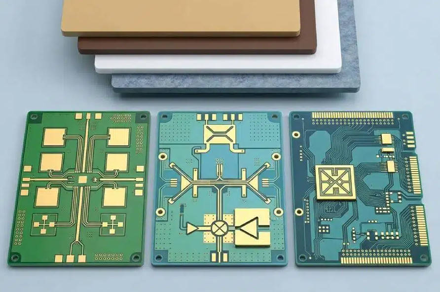
This is especially important when using RF laminates, PTFE-based materials, ceramic-filled materials, or hybrid stackups.
For controlled impedance RF PCBs, dielectric thickness tolerance is often as important as trace width tolerance.
A manufacturer should be able to review the stackup before production and confirm whether the selected material thickness and lamination structure can support the required impedance target.
3. Copper Thickness and Plating Tolerance
Copper thickness affects both electrical and manufacturing performance. In high-frequency applications, copper thickness influences trace geometry, impedance, conductor loss, and current handling.
Copper thickness can vary because of:
- Base copper tolerance
- Electroplating process
- Pattern plating
- Surface finish process
- Etching compensation
- Finished copper requirements
For RF traces, the final copper thickness should be considered during impedance calculation. If the design assumes one copper thickness but production results in another, impedance may shift.
Via plating thickness is also important. In high-frequency PCB manufacturing, vias may serve not only as interconnects but also as grounding structures, via fences, shield connections, or RF transitions. Poor plating consistency may increase reliability risk or degrade grounding performance.
4. Hole Size and Drill Position Tolerance
Drilling accuracy affects vias, mounting holes, plated through holes, and RF transition structures. In high-frequency PCB designs, via placement can influence grounding, shielding, return path continuity, and signal transitions.
Important drilling-related tolerances include:
- Drill diameter tolerance
- Finished hole size tolerance
- Drill-to-copper clearance
- Via position accuracy
- Annular ring tolerance
- Plating thickness
- Aspect ratio capability
RF and microwave boards often use ground via fences around transmission lines, filters, antennas, or shielded structures. If via position is inconsistent, the grounding structure may not perform as intended.
For high-speed and high-frequency boards, drill misregistration may also create reliability problems, especially when clearance is tight.
5. Layer Registration Tolerance
Layer registration describes how accurately different PCB layers align during fabrication. In multilayer high-frequency PCBs, layer alignment is important because signal layers, reference planes, buried structures, and via connections must match the intended design.
Poor registration can affect:
- Controlled impedance
- Plane alignment
- Via-to-pad reliability
- RF shielding structures
- Stripline geometry
- Differential pair behavior
- Layer-to-layer signal transitions
Layer registration is especially important in multilayer RF PCBs, hybrid stackups, and boards with buried or blind via structures.
When selecting a manufacturer, buyers should confirm whether the supplier can handle the required layer count, material combination, and registration control for the project.
6. Lamination Tolerance and Material Stability
Lamination is a key process for high-frequency PCBs. During lamination, pressure, temperature, resin flow, and material behavior determine final board thickness and layer bonding quality.
High-frequency laminates may behave differently from standard FR-4. Some materials may have different thermal expansion properties, resin content, or mechanical stability. Hybrid stackups can be more challenging because they combine materials with different characteristics.
Lamination variation can lead to:
- Thickness deviation
- Warpage
- Delamination risk
- Impedance variation
- Registration shift
- Unstable dielectric spacing
- Mechanical reliability issues
For RF and microwave applications, lamination control is not only a mechanical concern. It directly affects stackup accuracy and signal consistency.
Mars-PCB provides information about high-frequency RF PCB solutions for projects where material selection, stackup review, and manufacturing control need to be considered together.
How Different Tolerances Affect RF Performance
| Manufacturing Tolerance | Related PCB Feature | RF/Microwave Performance Risk |
| Line width tolerance | Microstrip, stripline, RF traces | Impedance shift, reflection, mismatch |
| Line spacing tolerance | Coupled lines, filters, differential structures | Coupling variation, crosstalk, frequency response shift |
| Dielectric thickness tolerance | Signal-to-plane distance | Impedance change, phase variation |
| Copper thickness tolerance | Trace geometry and conductor behavior | Impedance and loss variation |
| Drill tolerance | Vias, grounding, RF transitions | Weak return path, transition discontinuity |
| Layer registration tolerance | Multilayer stackup alignment | Stripline geometry error, via reliability issues |
| Lamination tolerance | Finished thickness and dielectric spacing | Stackup inconsistency, warpage, RF variation |
| Surface finish variation | Pads and exposed copper areas | Assembly and contact reliability concerns |
This table shows why high-frequency PCB manufacturing requires a wider process view. The issue is not one single tolerance, but how multiple small deviations combine.
Controlled Impedance Tolerance in High-Frequency PCB Manufacturing
Controlled impedance is one of the main reasons high-frequency PCB tolerances need strict attention. Impedance depends on several variables working together:
- Trace width
- Trace thickness
- Dielectric thickness
- Dielectric constant
- Solder mask condition
- Reference plane structure
- Copper roughness
- Fabrication process variation
In many PCB projects, impedance tolerance may be specified by the customer based on application requirements. The exact acceptable tolerance depends on circuit function, frequency range, design margin, and testing requirements.
A PCB manufacturer should not treat impedance as a simple number printed on a drawing. It requires stackup confirmation, material verification, process compensation, and sometimes impedance test coupons.
Controlled impedance tolerance should be reviewed before production, not only measured after boards are finished.
For buyers, this means the quotation stage should include enough information for the manufacturer to check impedance feasibility.
Standard PCB Tolerances vs High-Frequency PCB Tolerances
| Area | Standard PCB Concern | High-Frequency PCB Concern |
| Line width | Electrical connection and manufacturability | Impedance, loss, matching, RF response |
| Hole size | Component fit and plating reliability | Via transition, grounding, shielding, return path |
| Dielectric thickness | Finished board structure | Impedance and phase consistency |
| Copper thickness | Current capacity and fabrication | RF conductor behavior and impedance calculation |
| Layer registration | Connectivity and assembly reliability | Multilayer RF geometry and plane alignment |
| Lamination | Mechanical bonding | Stackup accuracy and RF signal consistency |
| Testing | Open/short testing | Electrical testing plus impedance and RF-related review when required |
| Material | Cost and mechanical needs | Dielectric constant, dissipation factor, thermal behavior |
This difference explains why buyers should not evaluate RF PCB manufacturing using only standard PCB purchasing criteria.
What Buyers Should Provide to Control PCB Tolerance Risk
A PCB manufacturer can only control tolerance risk effectively when the design information is clear. Buyers should avoid sending incomplete files and expecting the supplier to guess the electrical requirements.
Before quotation, prepare the following information:
| Information | Why It Helps |
| Gerber files | Defines trace geometry, copper layout, pads, planes, and routing |
| Drill files | Defines via size, hole position, and plated hole requirements |
| Stackup drawing | Helps evaluate dielectric thickness and impedance structure |
| Material specification | Determines dielectric behavior and manufacturing method |
| Copper thickness | Needed for impedance and fabrication planning |
| Finished board thickness | Important for mechanical and RF stackup control |
| Controlled impedance requirements | Helps the manufacturer review trace geometry and testing needs |
| Tolerance requirements | Clarifies critical dimensions and process expectations |
| Surface finish | Affects assembly, solderability, and sometimes RF considerations |
| Quantity and production stage | Helps distinguish prototype, pilot run, and production requirements |
For custom RF and microwave PCB projects, buyers can review Mars-PCB high frequency PCB services when preparing Gerber files, stackup information, and quotation requirements.
Common Mistakes When Managing High-Frequency PCB Tolerances
Mistake 1: Only Specifying Material, Not Stackup
Some buyers only specify the RF material name but do not provide a clear stackup. This is risky because material alone does not define impedance. Dielectric thickness, copper thickness, and layer structure are also required.
Mistake 2: Ignoring Finished Copper Thickness
The designed trace width may be calculated based on a certain copper thickness. If finished copper thickness differs from the design assumption, impedance may change. This should be reviewed before production.
Mistake 3: Treating RF Traces Like Normal Signal Lines
RF traces often require special attention to geometry, reference planes, solder mask, and spacing. They should be clearly identified when communicating with the manufacturer.
Mistake 4: Leaving Impedance Requirements Unclear
If impedance targets are not specified clearly, the manufacturer may produce the board according to Gerber geometry only. The result may be mechanically correct but electrically different from the design intention.
Mistake 5: Selecting a Supplier Based Only on Price
Low price is attractive, but high-frequency PCB projects often depend on process control, material handling, engineering review, and inspection. A cheaper board may become more expensive if it causes redesign, testing delays, or production failure.
How to Choose a Manufacturer for Tight High-Frequency PCB Tolerances
When evaluating a PCB manufacturer, buyers should look beyond basic capability lists. A supplier should be able to discuss how tolerances are managed throughout fabrication.
Key questions include:
- Does the manufacturer have experience with RF and microwave PCB materials?
- Can the supplier review controlled impedance before production?
- Can they support the required line width, spacing, hole size, and board thickness?
- Do they understand hybrid stackup lamination risks?
- Can they identify tolerance risks during DFM review?
- Can they provide impedance test discussion when required?
- Do they ask for complete Gerber, drill, material, and stackup files?
- Can they communicate clearly about process limits?
A suitable manufacturer should help identify manufacturability risks early. This is especially important for prototypes, where design validation and process feedback are both valuable.
You can use Mars-PCB as a reference when preparing high-frequency PCB project information and discussing custom manufacturing requirements.
Engineering Tips for Better Tolerance Control
Designers and buyers can also reduce tolerance-related risk by preparing the design properly.
Practical Design and Procurement Tips
| Tip | Benefit |
| Define controlled impedance traces clearly | Helps the manufacturer identify critical RF paths |
| Provide a complete stackup | Reduces assumptions during quotation and production |
| Confirm material availability early | Avoids last-minute substitution risk |
| Avoid unnecessarily tight tolerances | Helps control cost and improve manufacturability |
| Use realistic trace width and spacing | Supports stable etching and repeatable production |
| Discuss solder mask around RF traces | Prevents unexpected dielectric influence in sensitive areas |
| Validate prototypes before volume production | Reduces risk before larger orders |
| Communicate application requirements | Helps the supplier understand performance priorities |
Good tolerance control starts before fabrication. It begins with design clarity, manufacturability review, and accurate supplier communication.
FAQ
1. What are high frequency PCB tolerances?
High frequency PCB tolerances are the acceptable variations in line width, spacing, dielectric thickness, copper thickness, hole size, layer registration, lamination, and impedance during PCB manufacturing. These tolerances affect RF and microwave signal performance.
2. Why do PCB manufacturing tolerances matter for RF applications?
PCB manufacturing tolerances matter for RF applications because small dimensional changes can shift impedance, increase signal reflection, affect phase stability, or change insertion loss. RF circuits are more sensitive to geometry and material variation than low-speed circuits.
3. What tolerance affects controlled impedance in PCB manufacturing?
Controlled impedance is affected by trace width, copper thickness, dielectric thickness, dielectric constant, reference plane distance, solder mask condition, and fabrication consistency. These variables should be reviewed together during stackup and DFM evaluation.
4. How does dielectric thickness tolerance affect high-frequency PCB performance?
Dielectric thickness tolerance affects the distance between signal traces and reference planes. This can change impedance, phase behavior, and signal propagation. In RF and microwave PCBs, dielectric thickness control is critical for stable performance.
5. What should I send to a manufacturer for high-frequency PCB tolerance review?
You should send Gerber files, drill files, stackup drawing, material specification, copper thickness, finished board thickness, controlled impedance requirements, surface finish, quantity, and any critical tolerance requirements.
6. Is tighter PCB tolerance always better?
Not always. Tighter PCB tolerance can improve control for critical features, but it may also increase cost and manufacturing complexity. The better approach is to identify which dimensions are critical for RF performance and apply tighter control only where needed.
7. Can standard PCB manufacturers handle RF PCB tolerance requirements?
Some standard PCB manufacturers may handle simple RF boards, but demanding high-frequency or microwave PCBs often require experience with RF materials, impedance control, lamination behavior, and tighter process control. Supplier evaluation is important before production.
Conclusion
High frequency PCB tolerances play a direct role in RF and microwave circuit performance. Line width, dielectric thickness, copper thickness, drilling accuracy, layer registration, lamination stability, and controlled impedance all influence whether the finished board matches the design intention.
For buyers and engineers, tolerance control should be discussed before production, not after problems appear in testing. Complete design files, clear stackup information, material requirements, and impedance targets help the manufacturer evaluate manufacturability and reduce production uncertainty.
If your project involves RF communication, microwave circuits, antenna systems, radar modules, or high-speed signal transmission, you can review high frequency PCB manufacturing solutions from Mars-PCB and prepare your Gerber files for quotation.