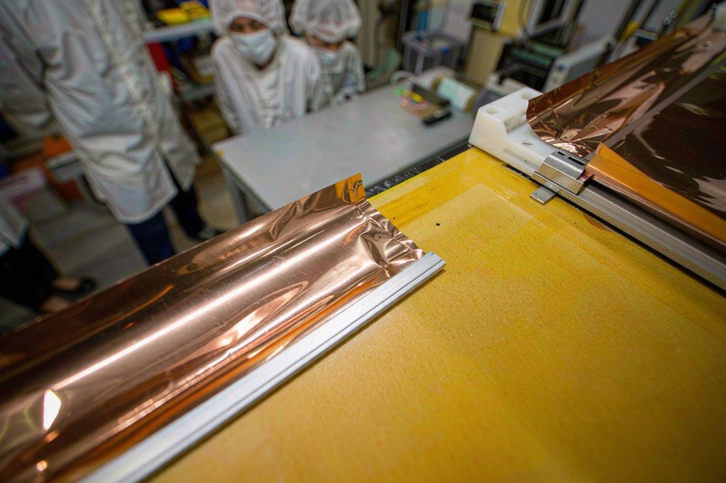
High frequency PCB lamination is the controlled process of bonding RF cores, copper layers, prepregs, and bonding films into a multilayer structure while maintaining dielectric thickness, layer registration, adhesion, and board flatness.
The most important point is that there is no universal lamination cycle for every high-frequency PCB.
A hydrocarbon-ceramic Rogers laminate, a ceramic-filled PTFE material, a woven-glass PTFE laminate, and a Rogers–FR4 hybrid stackup may require different bonding materials, temperature profiles, pressures, surface treatments, and cooling methods.
A process that works for a conventional FR4 multilayer board may cause excessive resin flow, insufficient fill, layer movement, weak adhesion, or dimensional instability when applied directly to a PTFE or mixed-material construction.
Successful RF PCB lamination begins with matching the press cycle to the exact laminate, bonding material, copper distribution, and stackup—not simply to the word “Rogers.”
This article follows the lamination process from stackup engineering through press cooling, identifying where manufacturing problems usually begin and how they can be controlled.
First Decision: Identify the Material System
“High-frequency material” is not one manufacturing category. Even within one supplier’s product portfolio, different resin systems behave differently during fabrication.
Rogers describes the RO4000 family as hydrocarbon-ceramic materials designed to provide high-frequency performance while using processing methods similar to standard epoxy-glass fabrication. In contrast, the RO3000 family consists of ceramic-filled PTFE composites and is processed using PTFE-compatible methods. (罗杰斯公司)
| Material System | General Processing Behavior | Typical Lamination Considerations |
|---|---|---|
| Standard FR4 | Thermoset epoxy-glass system | Familiar prepreg flow and conventional multilayer press cycles |
| RO4000-type thermoset laminate | More compatible with FR4-style processing | Requires suitable RO4400-series bondply or another approved bonding system |
| Ceramic-filled PTFE | Softer and processed as a PTFE material | Requires careful handling, adhesive selection, dimensional control, and cooling |
| Woven-glass PTFE | Better dimensional support than unreinforced PTFE | Still requires PTFE-compatible bonding and hole-wall processing |
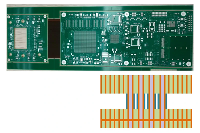
| Rogers–FR4 hybrid | Combines different material systems | Requires compatible cure temperatures, resin flow, thickness planning, and stackup symmetry |
| All-RF multilayer | RF material used throughout the stackup | Greater control over electrical properties but often higher processing complexity |
This classification should be completed before the press cycle is developed. A purchase order that specifies only “Rogers PCB” leaves too many variables undefined.
The quotation and stackup should identify:
- Exact laminate manufacturer and grade
- Core thickness
- Copper foil type and thickness
- Bondply, prepreg, or bonding film
- Number of bonding plies
- Finished dielectric thickness
- Required impedance
- Sequential lamination requirements
- Finished board thickness and tolerance
For projects involving RF transmission lines, filters, antennas, or microwave structures, these items should be reviewed before the layout is released to fabrication.
What Happens During High-Frequency PCB Lamination?
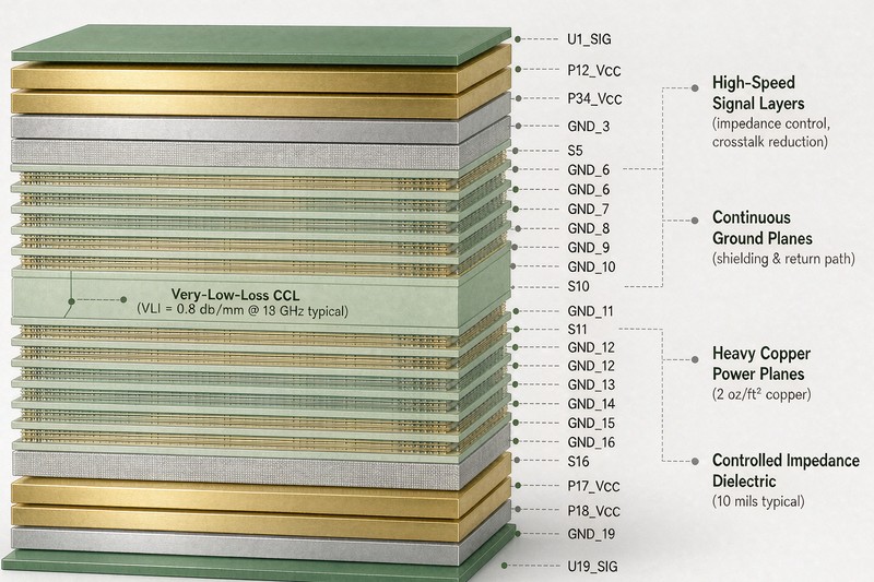
Lamination does more than hold the layers together. It establishes the physical dielectric structure used by the electrical model.
A typical multilayer process includes:
- Inner-layer imaging and etching
- Copper and dielectric surface preparation
- Baking to remove moisture and process volatiles
- Layup of cores, bondply, copper foil, and tooling materials
- Vacuum evacuation and initial pressure
- Controlled heating through the resin-flow window
- Full bonding or curing under pressure
- Controlled cooling
- Panel stabilization and dimensional inspection
- Drilling, hole-wall preparation, and plating
The exact sequence varies with the material and bonding system.
For RO3000 and RO3200 multilayer constructions, Rogers states that the inner layers should be baked before bonding to remove volatile substances. The press cycle is then determined by the selected adhesive system, and cooling under pressure is required when meltable thermoplastic films are used. (罗杰斯公司)
The laminated dielectric thickness is part of the RF circuit. A small manufacturing change can alter impedance, coupling, phase delay, filter response, or antenna resonance.
This is why a high-frequency stackup should not be treated as a nominal arrangement of materials. It must be treated as a controlled manufactured structure.
Failure Point 1: Choosing the Wrong Bonding Material
The bonding layer influences adhesion, finished thickness, resin flow, electrical loss, thermal resistance, and compatibility with later assembly cycles.
Common bonding options include:
- Thermoset RF bondply
- Standard or low-loss prepreg
- Thermoplastic bonding film
- FEP film
- PTFE fusion bonding
- Hybrid prepreg systems
The correct option depends on which surfaces are being joined and whether the bonding layer sits inside a critical RF field.
For RT/duroid 5870 and 5880 multilayers, Rogers distinguishes between thermoplastic and thermoset adhesive systems. Thermoplastic films may be selected where the electrical properties of the bonding layer are critical, while thermoset systems such as FR4 prepreg may be considered where those properties are less important. (罗杰斯公司)
Why Bonding Material Selection Goes Wrong
A material may be selected because it is:
- Already available in the factory
- Easy to press
- Lower in cost
- Compatible with an existing FR4 cycle
- Similar in nominal dielectric constant
However, these reasons do not confirm that it is suitable for the finished RF structure.
A bonding layer with excessive loss may reduce stripline performance. A film with an unsuitable remelt temperature may soften during later thermal processing. A low-resin prepreg may fail to fill around heavy copper features.
Practical Solution
Confirm the following before releasing the stackup:
- Bonding material designation
- Nominal and pressed thickness
- Dielectric constant and dissipation factor
- Resin content
- Copper-fill capability
- Cure or melt temperature
- Compatibility with sequential lamination
- Compatibility with lead-free assembly temperatures
- Whether the material is positioned in a critical RF field
Do not approve an impedance calculation that lists the RF core but omits the bonding layer.
Failure Point 2: Insufficient Resin Fill and Lamination Voids
Voids may form when air or process volatiles remain trapped between layers or when the bonding material cannot flow into low-pressure areas.
Likely contributors include:
- Inadequate vacuum
- Excessively fast heating
- Contaminated surfaces
- Moisture or residual chemicals
- Insufficient bondply resin
- Unbalanced copper patterns
- Deep etched features
- Large plane areas that restrict venting
- Pressure applied at the wrong stage
- Local areas surrounded by stacked copper features
RO4400 processing guidance notes that the actual thickness added by a bonding ply depends partly on the weight and distribution of copper. It also recommends careful venting-pattern design and warns against vertically stacked structures around low-pressure areas. (罗杰斯公司)
Void-Control Actions
| Risk | Engineering Response |
|---|---|
| Air trapped in low-pressure areas | Add suitable venting paths and use a validated vacuum cycle |
| Insufficient resin over etched copper | Increase resin content or use additional bonding plies |
| Plane-over-plane construction | Review resin access and local pressure distribution |
| High copper thickness | Recalculate fill demand rather than using a standard prepreg assumption |
| Rapid temperature rise | Slow the ramp through the resin-flow region where appropriate |
| Moisture or process chemicals | Bake and dry the inner layers according to the material system |
| Local copper imbalance | Add approved copper balancing or modify panel-level features |
A void problem is often a stackup and copper-distribution problem before it becomes a press problem.
Adding more pressure alone does not necessarily solve it. Excessive pressure may squeeze out too much resin, increase dielectric variation, or move thin cores.
Failure Point 3: Dielectric Thickness Variation
In an RF PCB, the distance between a signal trace and its reference plane directly affects impedance. The dielectric layer after pressing may not equal the nominal unpressed prepreg thickness.
Its final value depends on:
- Resin content
- Glass style
- Copper thickness
- Percentage of copper remaining after etching
- Local copper distribution
- Number of bonding plies
- Pressure
- Temperature profile
- Resin-flow characteristics
- Panel position within the press book
Rogers’ RO4400 guidance explains that pressed bondply thickness depends on the copper weight and copper distribution on the inner-layer surfaces. It also states that additional bonding material may be needed when the copper-fill requirement exceeds the capacity of the selected ply configuration. (罗杰斯公司)
Why Nominal Stackups Fail
A designer may calculate 50-ohm impedance using a nominal 0.10 mm dielectric layer. After pressing, resin flows into surrounding etched areas, leaving a different effective dielectric thickness under the trace.
The board may still pass a general finished-thickness inspection while the local RF geometry has moved outside the intended model.
Practical Solution
The manufacturer should calculate the stackup using:
- Pressed dielectric thickness
- Actual copper thickness after plating
- Selected material’s design Dk
- Intended trace width
- Copper roughness assumptions
- Solder mask influence where relevant
- Manufacturing etch compensation
The factory should also use impedance coupons representative of the actual layer construction.
Buyers can review high-frequency PCB manufacturing capabilities before sending the final stackup and impedance table for DFM evaluation.
Failure Point 4: Layer Registration and Dimensional Movement
Thin PTFE-based cores can be more flexible and easier to distort than conventional rigid laminates. Rogers’ RO3000 processing guidance notes that PTFE-based materials are softer than many other rigid PCB laminates and that thin cores can be creased or dimensionally distorted through improper handling. (罗杰斯公司)
Registration errors may appear as:
- Inner-layer shift
- Misaligned RF ground clearances
- Incorrect annular rings
- Via-to-pad offset
- Antenna geometry displacement
- Misalignment between coupled structures
- Incorrect layer-to-layer phase relationships
Common Causes
- Supporting a thin panel from one corner
- Mechanical scrubbing
- High roller pressure
- Inadequate tooling strategy
- Excessive press movement
- Poorly balanced copper
- Uncompensated material shrinkage
- Reusing FR4 compensation data for PTFE materials
Practical Solution
A controlled process may include:
- Flat tray transport for thin cores
- Chemical cleaning instead of aggressive mechanical scrubbing
- Material-specific X/Y compensation
- Post-etch measurement
- Optical or X-ray registration verification
- Suitable tooling holes and pinning strategy
- Copper retained around tooling areas where appropriate
- Prototype panel data used to refine production compensation
The compensation values should come from the exact material, thickness, copper pattern, and factory process—not from a generic material-family assumption.
Failure Point 5: Weak Interlayer Adhesion
Adhesion problems can originate long before the press closes.
Possible causes include:
- Fingerprints, oil, or dust
- Oxidized or degraded bondply
- Incorrect oxide treatment
- Inadequate copper surface preparation
- Mechanical damage to the exposed PTFE surface
- Insufficient drying
- Incorrect cure profile
- Incompatible bonding materials
- Premature loss of resin flow
- Transfer cooling of a thermoplastic system
RO4400 bondply guidance recommends controlled storage, sealed packaging, clean handling, copper surface treatment, and pre-bond baking. It also notes that aged material showing yellowing or hardening should be discarded. (罗杰斯公司)
For some PTFE materials, the as-etched dielectric surface should be preserved. Rogers warns that disturbing the surface may create a need for additional sodium treatment before bonding. (罗杰斯公司)
Practical Solution
Control adhesion through a documented chain:
- Verify bonding-material shelf life.
- Store it under the specified conditions.
- Prevent dust and fingerprints during layup.
- Use the approved copper treatment.
- Avoid unnecessary scrubbing of exposed RF dielectric.
- Bake the cores using material-specific conditions.
- Record the actual material temperature, not only platen temperature.
- Confirm pressure timing and cure duration.
- Cool according to the adhesive system.
- Validate adhesion through coupons or representative cross-sections.
Failure Point 6: Delamination During Cooling or Assembly
A panel may appear properly bonded when it leaves the press but later delaminate during drilling, surface finishing, soldering, or thermal cycling.
For thermoplastic bonding systems, controlled cooling under pressure is especially important. Rogers’ RT/duroid guidance states that transfer cooling can result in delamination and recommends that cooling proceed under pressure for the referenced thermoplastic adhesive cycles. (罗杰斯公司)
Potential causes include:
- Releasing pressure too early
- Cooling too rapidly
- Uneven cooling across the panel
- Excess residual stress
- A bonding film that remelts during assembly
- Moisture trapped before lamination
- Material CTE mismatch
- Insufficient cure
- Contamination at the bond interface
Practical Solution
The manufacturer should validate:
- Material temperature throughout the press cycle
- Cooling rate
- Pressure maintained during cooling
- Glass transition or melt behavior
- Compatibility with later soldering temperatures
- Sequential lamination exposure
- Thermal stress after surface finishing
A lamination recipe should not be copied from one adhesive system to another simply because the core material is similar.
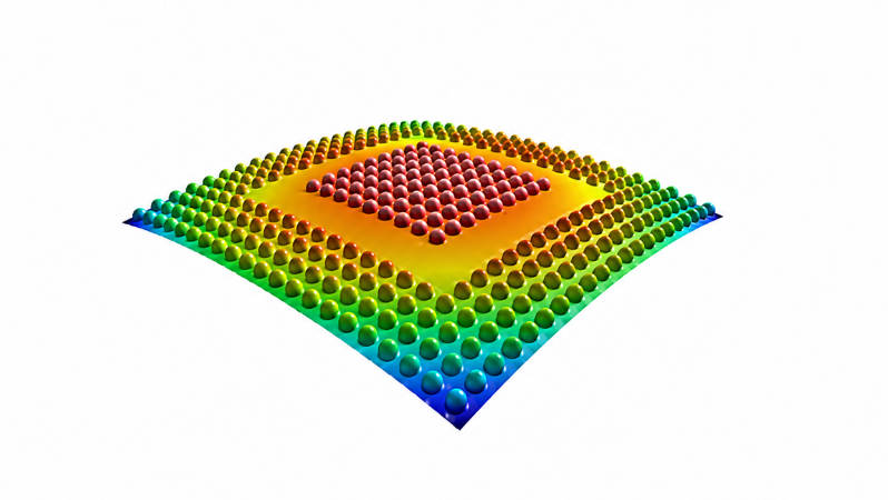
Failure Point 7: Bow, Twist, and Panel Warpage
Warpage occurs when the forces within the stackup are not balanced.
Frequent contributors include:
- Asymmetric layer construction
- Unequal copper distribution
- Different materials on opposite sides
- Unequal dielectric thicknesses
- Local heavy copper
- Uneven resin flow
- Incorrect press padding
- Uneven heating or cooling
- CTE differences in a hybrid structure
Hybrid boards are particularly sensitive because FR4, hydrocarbon-ceramic laminates, PTFE composites, copper, and bonding materials may expand differently.
Warpage-Control Strategy
- Use a mechanically balanced stackup where possible.
- Balance copper between corresponding layers.
- Avoid placing all RF material on one side without review.
- Use compatible bonding materials.
- Model the finished, not nominal, dielectric structure.
- Use appropriate press pads and separator materials.
- Control cooling uniformly.
- Measure panel flatness before routing.
- Review array layout and breakaway rails.
Warpage control should begin during stackup design; it cannot always be corrected after lamination.
PTFE, RO4000, and Hybrid Lamination Are Not the Same
| Process Issue | PTFE-Based Construction | RO4000-Type Construction | Rogers–FR4 Hybrid |
|---|---|---|---|
| Core handling | Often softer and more easily distorted | More rigid and FR4-like | Depends on the thinnest and softest layer |
| Bonding system | May use thermoplastic film, RF bondply, or approved prepreg | Often paired with RO4400-series bondply | Must be compatible with both material systems |
| Surface preparation | May require preservation or activation of PTFE surfaces | More compatible with conventional processes | Different surfaces may need different treatment |
| Press temperature | Highly dependent on adhesive or fusion-bond method | Typically compatible with thermoset processing | Must not damage or under-cure either system |
| Cooling | Critical for thermoplastic adhesives | Depends on selected bondply | Must control stress from material mismatch |
| Registration | Thin cores require additional support | Generally more stable | Compensation must account for both materials |
| Main risk | Distortion, adhesion, and thermoplastic process control | Resin fill and pressed-thickness variation | CTE mismatch, warpage, and incompatible cure conditions |
Rogers’ SpeedWave 300P guide illustrates why the exact bonding system matters: it specifies a controlled storage environment, vacuum pressing, defined pressure timing, a material-temperature cure requirement, and slow cooling for that particular hybrid multilayer prepreg. These values are product-specific starting points, not a universal recipe for every RF board. (罗杰斯公司)
A Failure Matrix for Engineering Reviews
| Observed Defect | Likely Process Causes | Items to Review |
|---|---|---|
| Lamination voids | Trapped air, inadequate venting, low resin content | Vacuum profile, copper pattern, bondply quantity |
| Resin starvation | Excessive flow or insufficient resin | Pressure, resin content, copper distribution |
| Excessive dielectric thickness | Insufficient pressure or limited resin flow | Press profile, copper fill, bondply selection |
| Low dielectric thickness | Excessive squeeze-out | Pressure timing, resin flow, edge dams |
| Inner-layer shift | Core movement or poor tooling | Pinning, handling, pressure application |
| Delamination | Contamination, incomplete cure, poor cooling | Surface treatment, cure record, cooling profile |
| Bow and twist | Asymmetry or thermal imbalance | Stackup, copper balance, cooling |
| Impedance outside tolerance | Pressed thickness or trace-width variation | Stackup data, etching, coupon results |
| Blisters after soldering | Moisture, volatiles, weak adhesion | Baking, storage, thermal validation |
| Inconsistent panel results | Uneven temperature or pressure | Press mapping, thermocouple data, book construction |
What the Manufacturer Needs Before Lamination Planning
A manufacturable RF stackup cannot be developed from Gerber files alone.
Provide:
- Exact laminate grade or approved alternatives
- Core and finished dielectric thicknesses
- Layer sequence
- Copper weights
- Finished board thickness
- Impedance requirements
- Frequency range
- Critical RF layers
- Bonding-material preference
- Surface finish
- Via structure
- Sequential lamination requirements
- Maximum bow and twist requirements
- Thermal and environmental conditions
- Prototype and production quantities
When a design is not yet finalized, an early RF PCB stackup review can identify material and lamination conflicts before the routing geometry is locked.
How to Evaluate a High-Frequency PCB Lamination Supplier
A supplier’s capability should be evaluated by process control rather than by a simple statement that it can manufacture Rogers boards.
Ask the following questions:
Material Control
- Will the quotation state the exact material grade?
- Are bonding materials traceable by lot and shelf life?
- Are substitutions approved before production?
- How are PTFE cores and bondply stored?
Stackup Engineering
- Does the impedance model use pressed dielectric thickness?
- Can the supplier recommend suitable bondply?
- Can it support pure RF and RF–FR4 hybrid structures?
- How are copper-fill requirements calculated?
Press Control
- Is vacuum lamination available?
- Are thermocouples used to verify material temperature?
- Are press cycles recorded by lot?
- How are pressure, ramp rate, dwell, and cooling controlled?
Dimensional Control
- Does the factory use material-specific compensation?
- Are thin RF cores mechanically supported?
- How is registration inspected?
- Is copper balancing reviewed during DFM?
Verification
- Are impedance coupons included?
- Can cross-sections be supplied?
- Are voids and resin fill inspected?
- Is finished board thickness measured by region?
- Are bow and twist inspected before shipment?
A supplier experienced in multilayer high-frequency PCB fabrication should be able to explain why a particular bondply and press approach fit the stackup rather than offering one fixed lamination cycle for every Rogers or PTFE board.
FAQ
What is high frequency PCB lamination?
High frequency PCB lamination is the process of bonding RF laminate cores, copper layers, and bonding materials into a multilayer board while controlling dielectric thickness, adhesion, registration, and flatness.
Is PTFE PCB lamination more difficult than FR4 lamination?
PTFE PCB lamination generally requires more specialized handling, surface preparation, bonding-material selection, and dimensional control. The exact difficulty depends on whether the PTFE is reinforced, ceramic-filled, or used in a hybrid structure.
What causes voids during RF PCB lamination?
Voids can be caused by trapped air, moisture, contamination, insufficient resin, poor venting, unbalanced copper patterns, or an unsuitable temperature and pressure profile.
Can standard FR4 prepreg be used with Rogers PCB material?
It may be used in some hybrid constructions, particularly where the bonding layer is outside the critical RF field. Suitability must be verified against electrical loss, cure compatibility, resin fill, thermal exposure, and the exact laminate grade.
How is dielectric thickness controlled in a multilayer RF PCB?
It is controlled through bondply selection, resin-content planning, copper-distribution analysis, press-cycle validation, material-temperature monitoring, and measurement of the finished construction.
Why does a Rogers PCB warp after lamination?
Warpage may result from an asymmetric stackup, uneven copper distribution, incompatible material expansion, nonuniform resin flow, or uneven heating and cooling.
Does every Rogers PCB use the same lamination process?
No. Rogers offers thermoset hydrocarbon-ceramic, ceramic-filled PTFE, woven-glass PTFE, and other material systems. Each must be processed according to its laminate and bonding-material requirements.
How can I verify an RF PCB supplier’s lamination quality?
Review material traceability, press records, impedance coupons, cross-sections, finished dielectric measurements, registration data, and bow-and-twist inspection results.
Conclusion
High frequency PCB lamination is not simply a higher-cost version of conventional FR4 pressing. It is a material-specific operation that determines the final electrical and mechanical structure of the RF board.
The most common problems—voids, resin starvation, dielectric variation, weak adhesion, inner-layer movement, delamination, and warpage—usually originate from an incompatibility between the stackup and the manufacturing process.
The most reliable workflow is to:
- Specify the exact RF material.
- Select a compatible bonding system.
- calculate the pressed stackup.
- Review copper distribution and resin fill.
- Develop a material-specific press cycle.
- Control heating, pressure, vacuum, and cooling.
- Validate the result through dimensional and electrical inspection.
Mars-PCB supports high-frequency and RF PCB manufacturing for projects involving controlled-impedance structures, specialized laminates, and multilayer stackups. For broader information about manufacturing and project coordination, visit Mars-PCB.