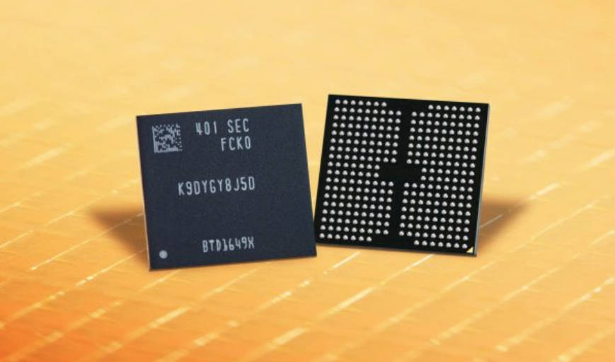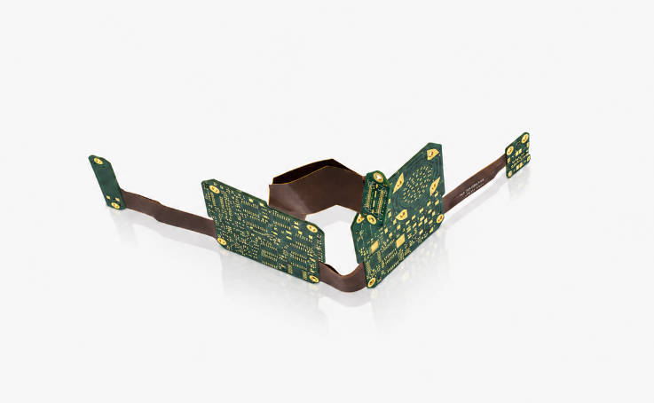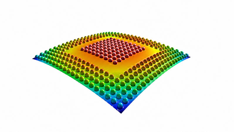
FC BGA substrate warpage is one of the most critical reliability challenges in advanced semiconductor packaging. As package sizes increase and substrate structures become thinner and more complex, controlling flatness becomes essential for stable assembly, reliable solder joints and long-term package performance.
FC BGA substrate warpage occurs mainly because of uneven material expansion, copper distribution imbalance, thin substrate structures and thermal stress during manufacturing and assembly processes.
A substrate that experiences excessive warpage may cause problems such as:
- poor die attach alignment;
- solder joint reliability issues;
- assembly defects;
- reduced manufacturing yield;
- long-term package reliability concerns.
For engineers working on advanced IC packaging, warpage control is not only a manufacturing issue. It starts from substrate design, material selection, stackup planning and process optimization.
This article explains the main causes of FC BGA substrate warpage and the practical methods used to improve substrate flatness and reliability.
Why FC BGA Substrate Warpage Matters
Flip-chip ball grid array (FC BGA) packages are widely used in high-performance semiconductor applications because they support:
- high I/O density;
- improved electrical performance;
- larger die sizes;
- advanced computing requirements.
However, FC BGA structures are becoming increasingly challenging.
Modern packages often require:
- thinner substrates;
- more routing layers;
- higher copper density;
- larger package dimensions.
These trends increase mechanical stress inside the substrate.
Impact of Excessive Warpage
| Problem | Possible Effect |
| Die attach misalignment | Reduced assembly accuracy |
| Uneven solder connection | Reliability risks |
| Poor package flatness | Assembly difficulties |
| Increased thermal stress | Long-term performance issues |
| Lower production yield | Higher manufacturing cost |
Maintaining IC substrate flatness is essential because even small deformation can affect precision semiconductor assembly processes.
What Causes FC BGA Substrate Warpage?
FC BGA substrate warpage is usually caused by a combination of material properties, structural design and manufacturing processes.
The most common factors include:
- CTE mismatch between materials;
- uneven copper distribution;
- multilayer stackup imbalance;
- thermal cycling stress;
- substrate thickness reduction;
- lamination process variation.
1. Material CTE Mismatch
Coefficient of thermal expansion (CTE) is one of the most important factors affecting substrate deformation.
Different materials expand and contract at different rates when temperature changes.
An FC BGA package may contain:
- substrate materials;
- copper layers;
- dielectric materials;
- solder materials;
- semiconductor die materials.
When these materials experience heating and cooling, different expansion rates generate internal stress.
CTE Mismatch Effect
| Material Combination | Potential Effect |
| Copper and dielectric | Internal stress generation |
| Substrate and die | Package deformation |
| Solder and substrate | Joint stress |
| Different dielectric layers | Uneven expansion |
A well-designed substrate structure must balance these material differences.
2. Copper Distribution Imbalance
Copper distribution is another major contributor to substrate warpage.
A multilayer substrate contains multiple copper patterns for:
- signal routing;
- power delivery;
- ground planes.
If copper density is significantly different between layers, internal stress becomes uneven.
Example of Copper Imbalance
| Design Condition | Warpage Risk |
| Balanced copper distribution | Lower deformation risk |
| Heavy copper on one side | Increased bending force |
| Uneven plane structures | Higher stress concentration |
| Large open areas | Possible dimensional instability |
Engineers should evaluate copper density during the layout stage rather than after fabrication problems occur.
3. Substrate Stackup Design
The layer structure of an FC BGA substrate directly affects mechanical balance.
A poorly balanced stackup may cause:
- bow;
- twist;
- uneven deformation.
Stackup Factors Affecting Warpage
| Factor | Influence |
| Number of layers | More layers increase complexity |
| Dielectric thickness | Affects mechanical stiffness |
| Copper layer arrangement | Controls stress balance |
| Symmetry | Improves flatness |
A symmetrical structure generally helps distribute mechanical stress more evenly.
4. Thermal Stress During Manufacturing
IC substrates experience multiple thermal processes, including:
- lamination;
- curing;
- solder reflow;
- assembly heating cycles.
Each thermal process can introduce stress.
During cooling, materials contract differently, which may create permanent deformation.
Manufacturing Stage and Warpage Risk
| Process Stage | Possible Cause |
| Lamination | Material shrinkage |
| Curing | Resin stress |
| Drilling | Local mechanical stress |
| Reflow | Thermal expansion mismatch |
| Assembly | Package-level stress |
Process control is therefore critical for maintaining substrate flatness.
Thin Substrate Design Challenges
Advanced semiconductor packages continue becoming thinner.
While thinner substrates provide advantages such as:
- smaller package profiles;
- reduced weight;
- better integration;
they also create additional warpage challenges.
A thinner structure has:
- lower mechanical stiffness;
- higher sensitivity to material stress;
- greater deformation possibility.
Thickness vs Warpage Relationship
| Substrate Condition | Effect |
| Thicker substrate | Higher rigidity |
| Thin substrate | More sensitive to stress |
| Large thin package | Higher warpage risk |
Designers need to balance miniaturization requirements with mechanical stability.
How to Control FC BGA Substrate Warpage
Warpage control requires cooperation between design, material selection and manufacturing processes.
1. Optimize Copper Balance
Copper balancing is one of the most effective approaches.
Recommended practices include:
- maintaining similar copper density between layers;
- avoiding extreme copper differences;
- reviewing large copper planes;
- applying dummy copper where appropriate.
The goal is to create a more mechanically balanced structure.
2. Improve Stackup Symmetry
A balanced stackup reduces uneven stress.
Engineers should evaluate:
- dielectric thickness;
- copper layer position;
- build-up sequence;
- layer symmetry.
Balanced vs Unbalanced Stackup
| Stackup Type | Result |
| Symmetrical structure | Better flatness control |
| Uneven layer arrangement | Higher deformation risk |
3. Select Appropriate Materials
Material selection strongly affects thermal behavior.
Important considerations include:
- CTE characteristics;
- dielectric properties;
- thermal stability;
- mechanical strength.
For advanced IC packaging, material compatibility is often more important than selecting a single high-performance material.
4. Control Lamination and Manufacturing Processes
Manufacturing consistency directly influences substrate flatness.
Important controls include:
- lamination pressure;
- temperature profile;
- curing conditions;
- dimensional inspection.
A stable manufacturing process helps reduce variation between production batches.
Mars-PCB provides IC substrate solutions designed for advanced semiconductor packaging requirements, including complex multilayer structures and high-density interconnect applications.
FC BGA Substrate Warpage Testing and Evaluation
Before mass production, substrate flatness should be evaluated through appropriate inspection methods.
Common evaluation considerations include:
- room temperature flatness;
- thermal deformation behavior;
- assembly condition simulation;
- package-level reliability testing.
Evaluation Focus
| Evaluation Item | Purpose |
| Flatness measurement | Check substrate deformation |
| Thermal analysis | Understand expansion behavior |
| Process simulation | Predict assembly risks |
| Reliability testing | Verify long-term stability |
Early evaluation helps identify design issues before production scaling.
Common Mistakes in Substrate Warpage Control
Mistake 1: Focusing Only on Material Selection
Warpage is not determined by material alone.
A good material can still experience deformation if:
- stackup is unbalanced;
- copper distribution is uneven;
- process control is insufficient.
Mistake 2: Ignoring Copper Density During Layout
Electrical routing decisions can affect mechanical performance.
Copper distribution should be considered together with electrical requirements.
Mistake 3: Reducing Thickness Without Structural Analysis
A thinner substrate may improve package size but increase deformation risk.
Mechanical simulation should be considered before reducing thickness.
Mistake 4: Evaluating Warpage Too Late
Fixing warpage problems after production begins can require expensive redesign.
Early collaboration between designers and substrate manufacturers is more effective.
FC BGA Substrate Selection Considerations
When selecting an IC substrate supplier, engineers should evaluate:
| Capability | Importance |
| High-density substrate experience | Supports advanced packages |
| Stackup design capability | Improves mechanical balance |
| Manufacturing process control | Reduces variation |
| Inspection capability | Ensures flatness |
| Prototype support | Enables early validation |
A capable supplier should understand both electrical requirements and mechanical reliability challenges.
For more information about substrate manufacturing capabilities, visit the Mars-PCB website.
Future Trends in FC BGA Substrate Development
As semiconductor technology advances, FC BGA substrates will continue facing increasing challenges:
- larger package sizes;
- higher layer counts;
- thinner structures;
- higher power density.
Future substrate solutions will focus on:
- improved warpage control;
- better material compatibility;
- advanced stackup optimization;
- higher manufacturing precision.
Warpage management will remain a key factor in achieving reliable semiconductor packaging performance.
FAQ
What causes FC BGA substrate warpage?
FC BGA substrate warpage is mainly caused by CTE mismatch, uneven copper distribution, stackup imbalance, thermal stress and thin substrate structures.
How can IC substrate warpage be reduced?
Warpage can be reduced through balanced copper distribution, optimized stackup design, suitable materials and controlled manufacturing processes.
Why is substrate flatness important for FC BGA packages?
Substrate flatness affects assembly accuracy, solder reliability and overall package performance.
Does thinner IC substrate increase warpage risk?
Yes. Thin substrates have lower mechanical stiffness and are generally more sensitive to thermal and structural stress.
How does copper distribution affect BGA substrate warpage?
Uneven copper distribution creates unbalanced internal stress, which can cause substrate bending or deformation.
What role does CTE play in IC substrate reliability?
CTE differences between materials create expansion and contraction stress during thermal cycles, influencing package deformation.