BGA Assembly
Mars PCB specializes in producing reliable BGA PCBs for today’s complex electronic devices.
BGA PCB: Understanding the Ball Grid Array in Modern Circuit Boards
Mars PCB specializes in producing reliable BGA PCBs for today’s complex electronic devices. With more than 15 years of industry expertise and three factories across China, our teams are equipped to handle the challenges of BGA manufacturing—from intricate routing to heat management—to ensure consistent quality and performance in your projects. These PCBs are vital to compact, high-performance electronics like computers, smartphones, and other advanced applications that demand space-saving designs and excellent thermal properties.
What is BGA in PCB?
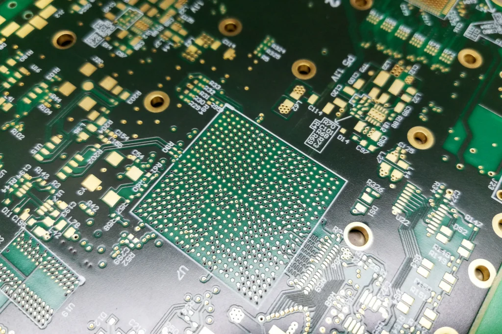
A ball grid array (BGA) refers to a type of surface mount packaging for integrated circuits. Instead of conventional pin connections, BGA PCBs rely on solder spheres beneath the IC. These solder balls allow for high-density connections required in modern electronics, leading to better heat conduction and more efficient use of board space. BGAs often appear in products like laptops, smartphones, and other devices where power efficiency and heat dissipation are crucial.
How Does a BGA PCB Differ from Other PCB Types?
By adding more components onto smaller boards, SMT helps push product designs to be lighter and sleeker. This density also lowers noise and signal delays, critical for higher-frequency circuits. In addition, automated assembly trims costs and speeds up production.
Key Components of a BGA PCB
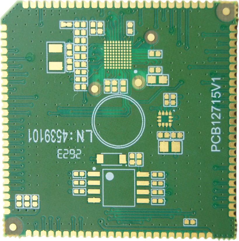
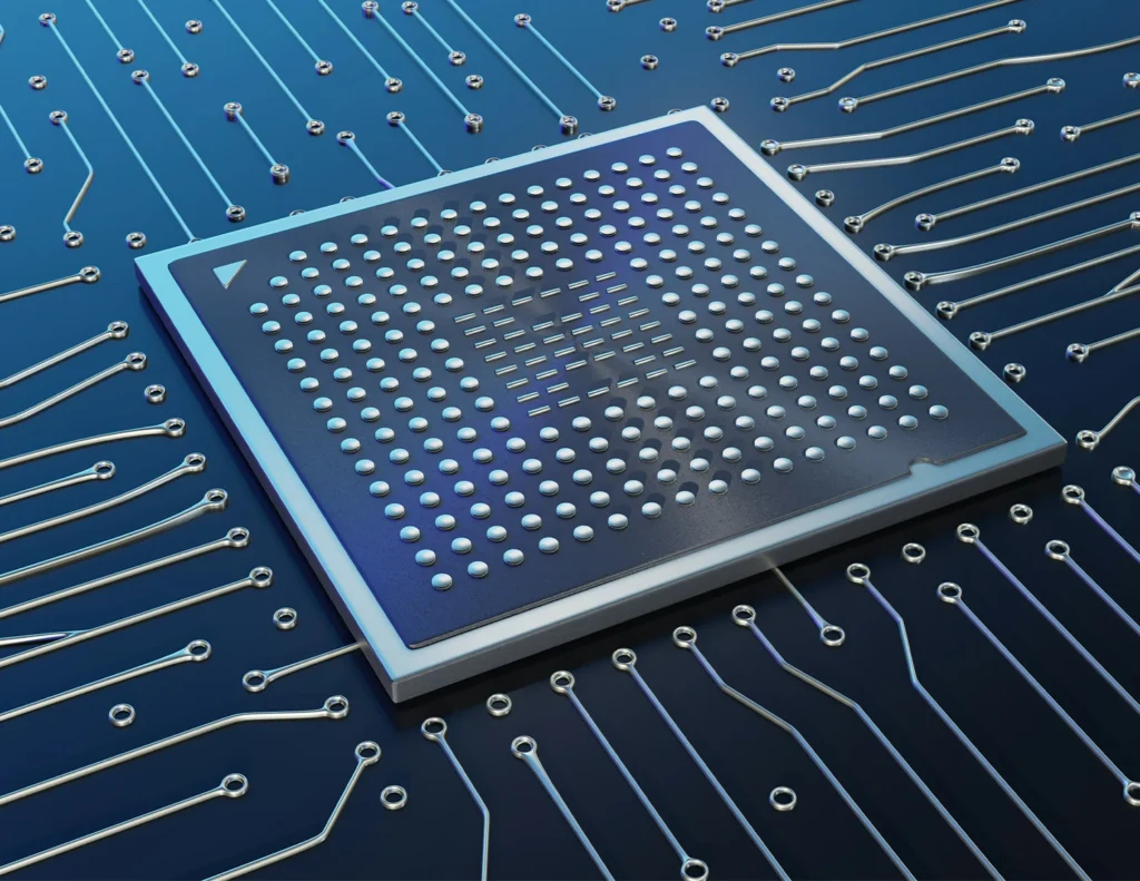
The integral component containing a grid of solder spheres on its underside for direct contact with the circuit board.
Typically made from resin-based materials (like FR-4), this layer supports the IC and links it to the solder spheres.
A protective layer over copper traces that prevents oxidation and unwanted solder bridging.
These tiny solder balls lie between the chip and the board, providing mechanical and electrical connections.
Positioned to align with the solder spheres on the package, allowing an electrical link between the board and the IC.
Copper traces route signals to and from components, while vias (tiny plated holes) connect layers in multi-layer boards.
BGA vs. CGA (Column Grid Array)
While both package types attach ICs onto PCBs, they differ in how connections are formed:
BGA | CGA | |
Connection | Uses round solder spheres to complete electrical contact between chip and board. | Employs tall, column-like leads that withstand higher heat loads. |
Advantages | Spheres become molten during reflow, offering higher-density interconnections for compact devices. | Metal columns have higher melt points, ensuring reliable connectivity under extreme temperatures. |
Use Cases | Ideal for consumer electronics, telecom, and high-speed applications needing compact footprints and quick heat flow. | Commonly employed in fields like aerospace and defense, where robust thermal performance and reliability are necessary. |
Benefits of Using BGA

With the ability to handle a large number of interconnections in a small area, BGA PCBs are indispensable in advanced telecommunications gear, high-performance servers, and consumer electronics.

BGA packages enable reduced connection lengths and excellent heat dispersal. Their short conduction paths help lower inductance, minimizing signal distortion in applications such as memory modules and processors.

Compared to older pin-grid arrays, BGAs use multiple solder spheres in grid form, allowing more circuitry in limited board space—a critical factor in miniaturized smartphones and portable gadgets.

Because of their composition and packaging, BGAs encourage quicker heat flow away from the chip, helping electronics run efficiently under heavy workloads.
Shorter interconnects and carefully designed board layouts help preserve clean signals at high frequencies, which is crucial for error-free data transfer.

Unlike long, thin pins that can bend or break, solder spheres distribute pressure across a grid, reducing damage from accidental knocks or thermal expansions.
Common Types of BGA Packages
Utilizes plastic as the main material, with a glass laminate or BT resin substrate. Cost-effective, suitable for moderate performance needs, but somewhat sensitive to humidity.
Built from layered ceramic with a metallic cover. Due to high-temperature solder spheres, they excel in thermal stability—ideal for advanced industrial or military applications.
Includes a cavity in the package for flexible designs, using either solder or lead bonding methods. Highly efficient in dissipating heat and often found in portable devices.
● Micro BGA: Miniaturized for extremely tight spaces.
● LGA (Land Grid Array): Uses contact pads or “lands” in place of solder spheres.
● POP (Package on Package): Stacks multiple BGA packages to save vertical space.
● Flip-Chip: Connects the die directly to the substrate, eliminating wire bonds.
● QFN: Features exposed pads on the bottom rather than spheres.
Selecting a BGA Package: Key Factors
Ensure your chosen package fits the available board space and meets your integration goals.
More pins mean more signal routes and power lines. Identify the complexity of your design needs before deciding on a BGA with a specific pin density.
Confirm the package’s ability to channel heat away—especially vital in high-power designs.
PBGA usually comes at a lower cost, while ceramic BGAs can be pricey yet outperform in extreme conditions.
Each field—be it automotive, telecommunications, or consumer electronics—may impose distinct endurance, performance, or compliance requirements.
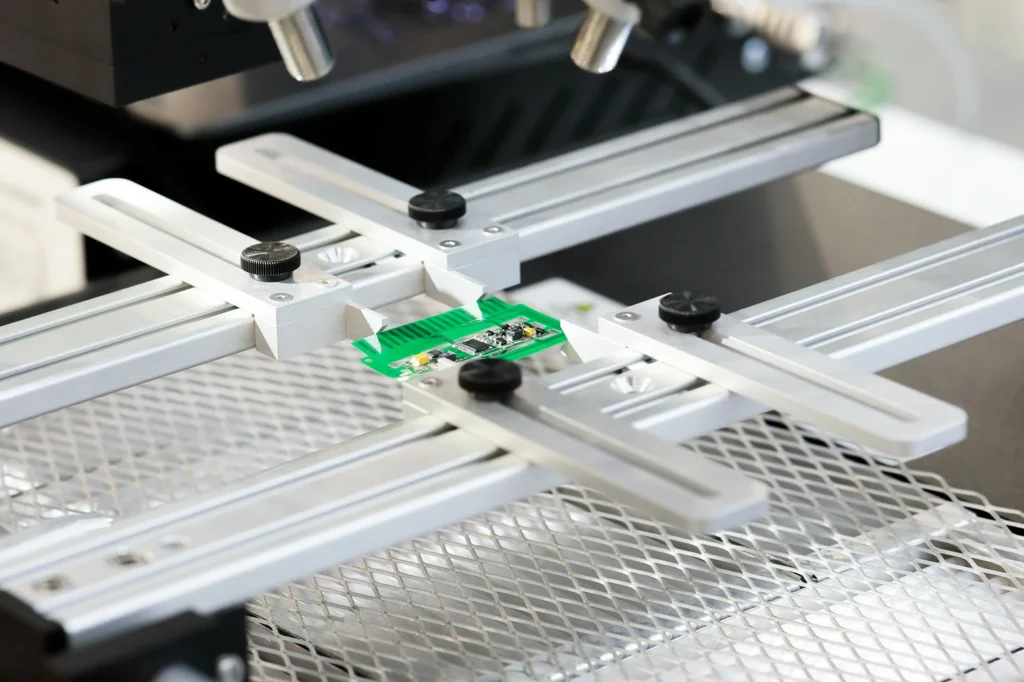
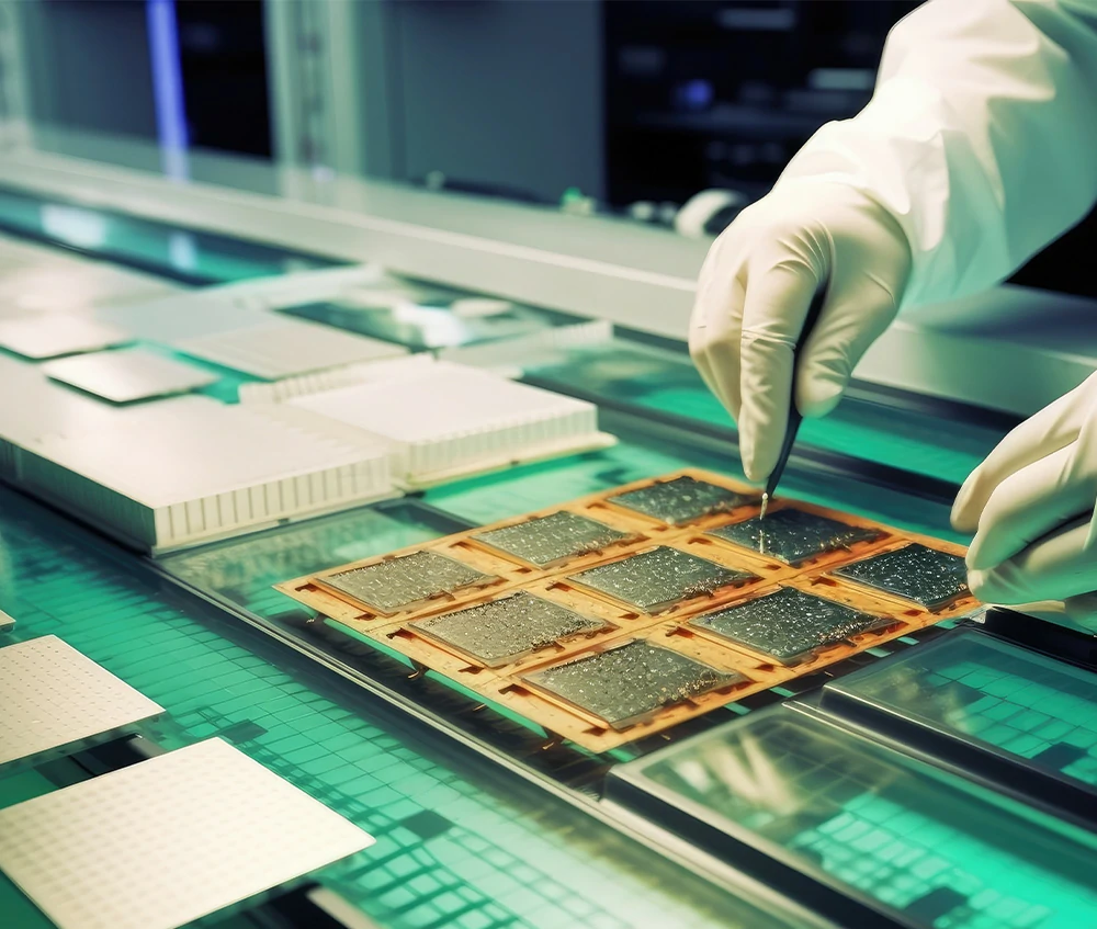
The BGA Manufacturing Process
Starting with resin-based materials (like FR-4), the substrate is cleaned and layered with copper. The IC is then attached using a conductive adhesive or bonding method, followed by wire bonding if needed.
Small solder spheres are aligned under the substrate in a precise grid pattern.
After applying solder paste to the circuit board, the BGA package is placed onto the PCB. In a reflow oven, the spheres melt, bonding the chip securely.
A specialized epoxy can be injected below the package if extra mechanical strength or heat conduction is necessary.
Residual flux or debris is cleared using solvents or water-based solutions to assure optimal component performance.
Techniques like X-ray and automated optical inspection verify solder joint integrity and alignment. Functional tests ensure the assembly meets performance benchmarks.
Materials Used in BGA Packages
PBGA: Plastic-based substrates (like BT resin) for cost-effectiveness.
CBGA: Multilayer ceramic with a metal enclosure for high-temperature stability.
TBGA: Polyimide films enabling unique, compact designs.
Tin-Lead Alloy: Lower melting points for simplified reflow.
Lead-Free: Tin-silver-copper variations, meet environmental standards with higher melting points.
Plastic or Ceramic Shells: Provide mechanical protection and manage heat dispersion.
Copper Traces: Conductivity and cost-effectiveness.
Gold-Plated Pads: Corrosion-resistant for consistent signal transmission.
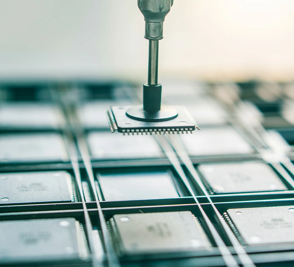
The BGA Assembly Process
Clean and coat the PCB with solder paste using a pre-made stencil to ensure precise application.
A high-accuracy pick-and-place machine positions the BGA package onto the board.
The solder melts in the oven, creating solid solder joints between the package spheres and the PCB pads.
Once cooled, the board is inspected for misalignments or bridging. Electrical tests confirm correct connectivity.
● Rework if needed, using heat-focused equipment to avoid damaging nearby parts.
● Cleaning again if flux residues remain.
● Coating or other protective methods if environmental protection is a concern.
Surface Mount Technology FAQs
The solder joints lie beneath the package, making defects or misalignments harder to detect. Also, reworking a BGA can be tricky because direct access to the solder spheres is limited.
● Signal Routing: Keep leads short for minimal signal interference, especially for high-speed paths.<br>
● Thermal Management: Allocate enough space for thermal vias, heatsinks, or airflow.<br>
● Accessibility: Leave a buffer zone around BGAs for inspection or repairs.
Layer count varies with pin numbers and design complexity. Simple low-pin BGAs may suffice with 2 to 4 layers, while complex, high-pin devices could require 6 or more. Discuss layer requirements with your manufacturer to ensure functionality and production feasibility.
Contact Our Team at Mars PCB
With a robust manufacturing capacity of 300,000 units per month and more than 500 skilled employees, Mars PCB is ready to handle your BGA PCB needs—from prototypes to large-scale orders. Our services cater to various sectors including automotive, communications, industrial, and medical fields.