Everything You Need to Know About Cavity PCBs: The Ultimate Guide
Quick Key Takeaways About Cavity PCBs
Feature | Benefit |
Recessed component placement | Reduces overall device size by up to 30% |
Improved component density | Allows 40% more components in the same footprint |
Enhanced signal integrity | Minimizes interference for critical RF applications |
Superior heat dissipation | Extends component lifespan by preventing overheating |


Introduction to Cavity PCBs
A Cavity PCB is a specialized printed circuit board featuring recessed areas that don’t fully penetrate the board. These cavities allow components to be mounted inside the board rather than on top, creating more compact and efficient electronic devices.
Unlike standard PCBs where components sit on the surface, cavity PCBs nest components within the board itself, making devices thinner while protecting sensitive parts and improving signal integrity.
With the growing demand for smaller, more powerful electronics, cavity PCB technology has become essential for 5G networks, IoT devices, automotive systems, and AI applications. Industry reports from Markets and Markets show demand growing approximately 12% annually since 2022.
Types of Cavity PCBs
Single-Sided Cavity PCBs
Single-sided cavity PCBs feature recessed areas on only one side of the board. This cost-effective design works well when you need to:
- Recess just a few taller components
- Maintain a flat surface on one side
- Keep manufacturing costs down
Common applications include consumer electronics, automotive dashboards, and smart home devices
Double-Sided Cavity PCBs
Double-sided cavity PCBs incorporate recessed areas on both sides, maximizing space efficiency for ultra-compact devices where components need protection on both sides. They’re ideal for portable devices where weight distribution and size are critical factors.
Multi-Layer Cavity PCBs
The most advanced cavity PCBs integrate cavities within complex stackups of 4, 6, 8 or more layers. These sophisticated structures enable extremely dense component placement and complex interconnections for high-performance applications.
Advantages of Cavity PCBs in Detail
Miniaturization and Space Efficiency
Research from the IPC indicates cavity PCB designs can achieve:
- 30-50% reduction in overall board height
- 15-25% reduction in total PCB footprint area
- 20-35% reduction in final product volume
These reductions create competitive advantages in markets where device size matters, such as wearables, medical implants, and aerospace applications.

Thermal Management Superiority
Heat is electronic components’ biggest enemy. Cavity PCBs offer superior thermal management by allowing components to directly contact heat sinks and creating shorter thermal paths. Testing shows properly designed cavity PCBs can achieve 15-30% lower peak component temperatures, extending product lifespan by 25% or more.
Enhanced Signal Integrity and Performance
By allowing components to be mounted closer together and to ground planes, cavity PCBs achieve shorter trace lengths, reduced parasitic effects, and minimized signal distortion. According to the IEEE Transactions on Components, cavity PCB designs can reduce signal path lengths by up to 40%.
Real-World Applications of Cavity PCBs

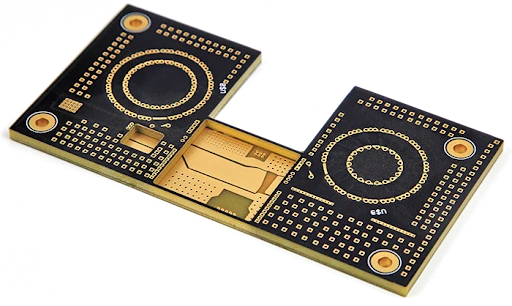
RF and Microwave Systems
At high frequencies, every millimeter of trace length dramatically affects performance. Cavity PCBs provide precise impedance control, minimized parasitic effects, superior isolation between signal paths, and reduced radiation losses.
Common applications include 5G equipment, satellite communications, automotive radar, and medical imaging devices.

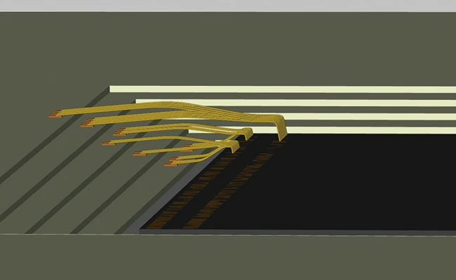
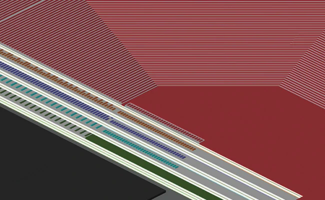
Telecommunications Infrastructure
For telecom applications, cavity PCBs deliver higher port density, improved signal integrity for high-speed data, better thermal management for continuously operating systems, and enhanced reliability for mission-critical applications.
You'll find this technology in network switches, optical conversion modules, server backplanes, and 5G base stations.

Automotive Electronics
Modern vehicles contain up to 100 electronic control units and thousands of components. Cavity PCBs help meet automotive challenges with improved vibration resistance, thermal cycling tolerance, and EMI compliance.
Key automotive applications include advanced driver assistance systems (ADAS), engine control modules, infotainment systems, and electric vehicle power management.

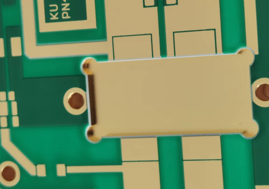
Power Electronics and Amplifiers
In power applications, cavity PCBs allow direct attachment of components to heat sinks, provide lower thermal resistance paths, and enable physical separation of high-voltage components.
Manufacturing Process of Cavity PCBs
Design and Engineering Phase
Creating effective cavity PCBs begins with careful design that considers both electrical and mechanical requirements, including:
- Component placement optimization
- Cavity dimension planning
- Layer stackup design
- Signal integrity simulation
- Thermal modeling
Material Selection and Precision Machining
Material selection significantly impacts performance, with options ranging from standard FR-4 to specialized Rogers or PTFE-based substrates for RF applications.
Cavity creation requires advanced machining with positional accuracy to within ±0.001 inches using CNC routing, milling, or laser ablation for the highest precision requirements.

Design Considerations for Optimal Performance
Cavity Dimensions and Tolerances
Critical dimensional factors include cavity depth to accommodate components while maintaining minimum dielectric thickness, appropriate clearances for component placement, and proper consideration of tolerance stack-up.
Material Selection Based on Application
Different applications require specific materials:
- RF and microwave: Low-loss materials like Rogers or PTFE-based substrates
- Power electronics: High thermal conductivity substrates or metal core PCBs
- Automotive/medical/aerospace: Materials with appropriate reliability ratings
Electrical Requirements and Signal Integrity
Maintaining signal integrity requires careful attention to impedance control, proper power distribution, and EMI/EMC considerations specific to cavity designs.

Industry Standards and Compliance (IPC)
Several IPC standards apply to cavity PCB manufacturing, including:
- IPC-2221/2222: General PCB design guidelines
- IPC-6012: Qualification and performance specifications
- IPC-4101: Base material specifications
- IPC-A-600: Acceptability criteria for finished PCBs
Adherence to these standards ensures quality, reliability, and compatibility across manufacturers.
Challenges and Solutions
Manufacturing Complexity
Creating consistent, high-quality cavity PCBs presents significant challenges in depth control, registration, and alignment. Solutions include adaptive machining, optical measurement systems, process monitoring, and specialized fixturing.
Cost Considerations
Cavity PCBs typically cost more than standard PCBs due to additional processing steps, higher material waste, and more stringent quality requirements. Cost management strategies include designing for manufacturability, standardizing cavity dimensions, and optimizing panel utilization.
Future Trends in Cavity PCB Technology
The PCB market is expected to grow by 5.5% in 2025, reaching US$85.4 billion, driven by AI servers and electric vehicles. For cavity PCBs, key trends include:
- Integration with additive manufacturing processes
- Advanced materials with improved thermal and electrical properties
- Automated design tools specifically for cavity PCB optimization
- Greater miniaturization with higher precision manufacturing


Why Choose MarsPcb for Your Cavity PCB Needs
As a world-leading PCB manufacturing and assembly company, MarsPcb offers:
- Advanced cavity PCB design consultation and DFM support
- State-of-the-art manufacturing equipment for precise cavity creation
- Comprehensive testing and verification procedures
- Experience across diverse applications from RF to automotive
- Complete turnkey service including component sourcing and assembly
FAQs About Cavity PCBs
Cavity PCBs reduce size and weight, increase assembly density, improve performance and reliability, and enhance heat dissipation, making them ideal for high-performance applications.
Manufacturing involves design and engineering, material selection, precision machining using CNC or laser technology, layer alignment and bonding, and circuit patterning and etching.
Cavity PCBs excel in RF/microwave systems, telecommunications, automotive electronics, power amplifiers, and high-speed computing applications where space, performance, and thermal management are critical.
They reduce signal path lengths, minimize parasitic effects, improve grounding, and enable better isolation between signal paths, resulting in enhanced performance for high-frequency applications.
How do cavity PCBs improve signal integrity?
They reduce signal path lengths, minimize parasitic effects, improve grounding, and enable better isolation between signal paths, resulting in enhanced performance for high-frequency applications.

Professional PCB & PCB Assembly Manufacturer & Factory
From concept to completion, your project will be under experienced project management, sparing you the hassle of untimely conference calls, communication gaps, language barriers and “real time” information gathering.