The relentless pace of innovation in electronics constantly pushes the boundaries of what’s possible. From the smartphones in our pockets to sophisticated medical implants, the demand for smaller, lighter, and more powerful devices is insatiable. This drive for miniaturization and superior performance often stretches the capabilities of traditional Printed Circuit Boards (PCBs) to their limits. While standard PCBs remain the workhorse of the industry due to their cost-effectiveness and widespread use, they frequently encounter hurdles when faced with complex modern requirements, particularly regarding component integration, thermal management, and maintaining signal integrity at high frequencies.
Enter Cavity PCBs – an advanced solution designed to overcome these very challenges. By enabling the embedding of components and creating specialized internal structures, cavity designs are becoming indispensable for next-generation electronic applications. This article will delve into a comparative analysis of Cavity PCBs and Standard PCBs, illuminating how the former addresses critical design limitations and unlocks unparalleled capabilities in today’s high-performance electronics.
Understanding Standard PCBs: The Foundation
At its core, a standard PCB is a flat laminate substrate, typically made of FR-4 (a glass-reinforced epoxy laminate material), with conductive traces etched onto its surface and internal layers. Components are then mounted onto these surfaces, predominantly using Surface Mount Technology (SMT).
| Feature | Description |
| Structure | Multi-layered with copper traces and dielectric material. |
| Materials | Predominantly FR-4, offering a good balance of cost and performance. |
| Manufacturing | Well-established, cost-efficient, and widely accessible processes. |
| Component Mount | Primarily surface-mount technology (SMT) on the external layers. |
While standard PCBs excel in cost-effectiveness, ease of manufacturing, and ubiquitous availability, their inherent design presents limitations for cutting-edge applications. Relying solely on surface-mounted components consumes valuable board real estate. Furthermore, managing heat from high-power components and maintaining precise signal integrity for high-frequency or high-speed digital signals can become increasingly difficult and costly on a standard board, often requiring additional external components or complex routing.
Deep Dive into Cavity PCBs: Design and Fabrication Principles
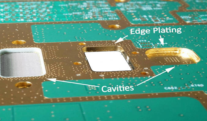
A Cavity PCB fundamentally differs from a standard board by incorporating precisely engineered depressions or “pockets” within its dielectric layers. These cavities are not just simple holes; they are meticulously formed spaces designed for specific purposes: to embed electronic components directly within the PCB stack-up, create controlled air gaps for impedance matching, or provide direct thermal pathways for heat dissipation.
Types of Cavities
Cavities can be categorized based on their depth and enclosure:
- Blind Cavities: These cavities are open on one side of the PCB stack-up but are enclosed by layers on the other side. They are ideal for embedding components that need to be accessed from one side for assembly or testing.
- Buried Cavities: Fully enclosed within the PCB’s internal layers, buried cavities offer maximum protection for embedded components, shielding them from environmental factors and mechanical stress.
- Through Cavities: Less common for component embedding, these cavities extend through the entire board thickness. They are often used for integrating large heat sinks or specialized connectors directly into the PCB structure.
Key Fabrication Processes for Cavities
The creation of cavities requires specialized and precise manufacturing techniques beyond standard PCB etching:
- Controlled Depth Routing/Milling: This involves using highly accurate CNC routers to remove material to a specified depth, forming the cavity. Precision is paramount to ensure consistent cavity dimensions.
- Laser Ablation: For extremely fine features and tighter tolerances, especially when dealing with advanced materials or very thin layers, lasers are employed to precisely ablate (vaporize) material.
- Press-Fit/Compression Molding: In some advanced cavity PCB manufacture processes, cavities are formed during the lamination stage by using molds or pre-formed dielectric materials that create the desired void.
The ability to control tolerances and depth with extreme accuracy is critical in cavity PCB manufacture to ensure the proper fit and performance of embedded components. Additionally, the integration of specialized materials, such as specific RF laminates or thermal management materials, around these cavities is often crucial for optimizing performance. For users looking for specific designs, Custom cavity PCB services allow for tailored solutions to meet unique application demands.
Cavity PCBs vs. Standard PCBs: A Comparative Analysis
The advantages of Cavity PCBs over standard PCBs become evident when we examine critical performance metrics for modern electronics.
| Feature | Standard PCBs | Cavity PCBs |
| Miniaturization | Components are surface-mounted, occupying valuable board real estate; limits density. | Enables component embedding, allowing for significantly smaller form factors, reduced overall Z-axis height, and higher component density. Ideal for ultra-compact devices. |
| Signal Integrity | Longer traces, vias, and surface routing can introduce more parasitic effects (inductance, capacitance), leading to signal degradation at high frequencies. | Shorter interconnects, direct connections, controlled impedance structures, and the ability to use air as a dielectric (achieved through controlled cavities) drastically reduce parasitics, improving signal performance for RF/Microwave and high-speed digital applications. |
| Thermal Management | Relies on thermal vias or external heat sinks, often less direct and efficient for high-power components. | Provides direct thermal paths from embedded components to external heat sinks or internal thermal planes, leading to significantly more efficient heat dissipation and improved component reliability. |
| Reliability/Ruggedness | Surface-mounted components are exposed to environmental factors (dust, moisture, shock, vibration). | Embedded components are physically protected within the PCB stack-up, enhancing overall system reliability, especially in harsh environments. |
| Cost | Generally lower initial cost due to simpler manufacturing processes and widely available materials. | Higher initial design and manufacturing complexity, requiring specialized equipment and expertise. Often results in a higher unit cost. |
| Manufacturing Process | Established, less complex, higher yield for general-purpose applications. | Requires advanced processes like controlled depth routing, laser ablation, and precise lamination; demands specialized cavity PCB manufacture capabilities. |
When precision, performance, and miniaturization are paramount, Cavity PCBs offer a clear advantage. While the upfront cost for a Custom cavity PCB or wholesale cavity PCB might be higher than a standard board, the long-term benefits – including enhanced performance, increased reliability, and the ability to achieve unprecedented levels of integration – often translate into overall system cost reductions and open doors for entirely new product categories. The value proposition extends beyond raw material cost to encompass the entire product lifecycle and market competitiveness.
Ideal Applications for Cavity PCBs
The unique capabilities of Cavity PCBs make them indispensable for a range of demanding applications:
- RF and Microwave Modules: In wireless communication, radar systems, and satellite technology, cavity PCBs are crucial for building high Q-factor filters, power amplifiers, and mixers. Their ability to minimize parasitic effects and control impedance precisely makes them superior for maintaining signal integrity at gigahertz frequencies.
- High-Speed Digital Boards: For data centers, servers, high-performance computing, and AI accelerators, cavity PCBs facilitate faster data transfer rates (multi-Gbps) by ensuring clean signal paths and reducing latency.
- Medical Devices: The extreme miniaturization capabilities of cavity PCBs are vital for implantable devices like pacemakers, neuro-stimulators, hearing aids, and other portable diagnostic tools where space is at a premium and reliability is non-negotiable.
- Automotive Electronics: In advanced driver-assistance systems (ADAS), infotainment, and engine control units, cavity PCBs contribute to robust, compact, and high-performance solutions capable of withstanding harsh automotive environments.
- Aerospace and Defense: For avionics, drone technology, and defense systems, the combination of light weight, high reliability, and excellent thermal management offered by cavity PCBs is critical for mission-critical applications.
Design and Manufacturing Considerations for Cavity PCBs
Adopting cavity PCB design requires a more integrated and meticulous approach than traditional PCB development:
- Early Design Collaboration: It is crucial for design teams to engage with a skilled cavity PCB manufacture partner early in the design cycle. Their expertise in material selection, process capabilities, and design for manufacturability (DFM) is invaluable.
- Material Selection: Choosing the appropriate dielectric materials, prepregs, and copper weights is paramount. Specialized low-loss or thermal management laminates may be required depending on the application’s electrical and thermal demands.
- IPC Standards and Guidelines: Adherence to specific IPC standards for advanced PCB fabrication (e.g., IPC-6012E, IPC-6018B for high-frequency applications) is essential to ensure quality and reliability.
- Simulation and Modeling: Advanced electrical and thermal simulation tools are indispensable for validating the pcb cavity design before physical prototyping. This helps in predicting performance, identifying potential issues, and optimizing the design.
- Test and Reliability: Specialized testing methods, including in-circuit test (ICT) and functional test (FCT), need to be adapted for boards with embedded components. Robust reliability testing (e.g., thermal cycling, shock, vibration) is also critical.
- Supply Chain for Wholesale Cavity PCB: For large-scale production, establishing a reliable supply chain for wholesale cavity PCB components and fabrication is crucial.
Conclusion: The Future is Embedded
Cavity PCBs represent a significant leap forward in printed circuit board technology, directly addressing the limitations of standard PCBs in an era of escalating performance and miniaturization demands. By enabling component embedding, superior thermal management, and unparalleled signal integrity, Cavity PCBs unlock critical capabilities for next-generation electronic products.For engineers and product developers grappling with the constraints of traditional PCB designs, exploring Cavity PCB solutions is not merely an option but a strategic imperative. The initial investment in Custom cavity PCB solutions or wholesale cavity PCB might be higher, but the long-term benefits in terms of enhanced product performance, increased reliability, reduced form factor, and ultimately, market competitiveness, are undeniable. As electronics continue to shrink and demand more from every component, the future of high-performance design is undeniably embedded.

