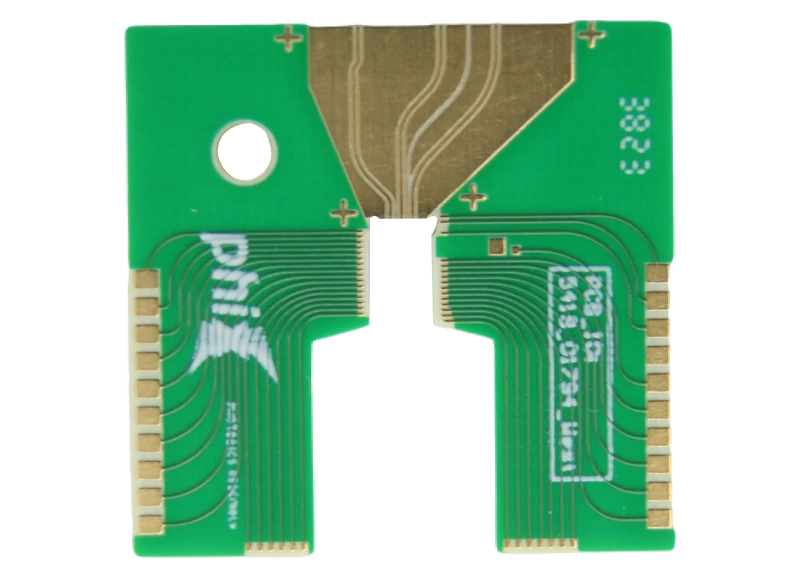
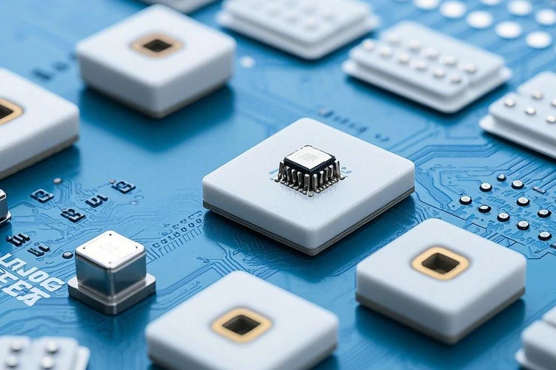
AlN and Alumina Substrate Ceramic PCB Manufacturing
Ceramic PCBs are made from advanced materials like aluminum nitride (AlN) and alumina, offering excellent thermal conductivity, electrical insulation, and low dielectric loss.
What is a Ceramic PCB?
A ceramic PCB consists of a ceramic material as the base, often combined with a binder to form a durable, heat-conductive layer. These boards are made from materials like alumina (Al₂O₃) or aluminum nitride (AlN), which are known for their high thermal conductivity. The core of ceramic PCBs is designed to efficiently dissipate heat from hotspots and distribute it evenly across the surface, ensuring optimal performance even under extreme conditions.
Unlike standard PCBs that use materials like fiberglass, ceramic PCBs are made with advanced manufacturing techniques like LAM (Laser Assisted Metallization) to print conductive pathways on ceramic substrates. This results in improved performance and simplified production for high-demand applications.
Why Ceramic PCBs Are a Top Choice
One of the main reasons ceramic PCBs are favored in the electronics industry is their outstanding thermal expansion properties. With a thermal conductivity that rivals silicon, ceramic materials act as both heat conductors and insulators, making them ideal for devices subjected to heat fluctuations.
Ceramic materials offer excellent stability and can endure harsh environments without losing performance. Their inherent resistance to chemical erosion and moisture makes them especially reliable for long-term use in electronic devices. Moreover, ceramic’s high durability ensures that the PCB will not wear down quickly, even in demanding applications.
Ceramic PCBs are incredibly versatile. Whether you are working with high-power modules or high-frequency circuits, ceramic boards offer both mechanical strength and heat resistance, making them perfect for applications across industries like automotive, telecommunications, aerospace, and more.
Ceramic boards, particularly those with metal cores, offer high mechanical stiffness, which is crucial for applications requiring robust performance under stress. This adaptability ensures that ceramic PCBs can perform optimally across a wide range of devices and environments.
Key Materials in Ceramic PCBs
When manufacturing ceramic PCBs, the choice of base material plays a crucial role in their performance.
Common materials include:
Alumina is one of the most widely used materials in ceramic PCBs due to its affordability, excellent thermal conductivity (25 W/(m.k)), and high electrical resistivity. It is commonly used in low-cost applications where high performance is still required.
For applications requiring superior thermal conductivity (up to 300 W/(m.k)), aluminum nitride is the material of choice. It’s used in high-power devices and systems that demand precise heat management. However, its higher cost can be a factor to consider for budget-conscious projects.
With exceptional thermal conductivity (up to 330 W/(m.k)), beryllium oxide is ideal for high-performance electronic components. Although it’s one of the more expensive ceramic materials, its unique properties make it indispensable in advanced applications.
Types of Ceramic PCBs
Ceramic PCBs are crucial for applications requiring high thermal conductivity, electrical insulation, and excellent reliability in extreme conditions. There are several types of ceramic PCBs, each tailored for specific uses and manufacturing processes. Below are the most common types of ceramic PCBs
High-Temperature Co-fired Ceramic (HTCC) PCBs are made by combining materials like aluminum oxide (Al₂O₃), plasticizer, lubricant, and solvent. The process involves rolling, forming, covering, and tracing circuits on refractory surfaces, such as tungsten. The PCB is then baked in a high-temperature oven (1600°C – 1700°C) for 32-48 hours. The HTCC process produces durable, high-performance boards but is more suitable for small-scale production due to the challenges of warping and shrinkage.
Applications:HTCC is typically used in aerospace, military, and medical electronics, where high-temperature stability and electrical performance are essential.
Key Features:
- High thermal and electrical performance
- Ideal for small-scale, high-temperature applications
- Difficult to scale for large production due to warping and shrinkage
Low-Temperature Co-fired Ceramic (LTCC) PCBs are made by mixing crystal glass, composite glass, and non-glass adhesive materials. The process involves forming sheets, circuit tracing with conductive gold paste, and baking the layers at lower temperatures (less than 1000°C). LTCC boards are commonly used in applications that require multi-layer interconnects and small size.
Applications:LTCC is widely used in telecommunications, automotive, and medical applications where high-density circuits and reliable electrical performance are needed.
Key Features:
- Multi-layer capability
- High-density interconnects
- Excellent shrinkage control and accurate circuit alignment
Direct Bonded Copper (DBC) PCBs involve bonding a copper foil directly to the ceramic substrate at high temperatures. This process ensures a thin and compact PCB with excellent solderability, high thermal conductivity, and strong bonding strength. DBC is known for its ability to handle high current and high-temperature applications.
Applications:Commonly used in power modules, automotive electronics, and LED lighting systems, where high power handling and heat dissipation are critical.
Key Features:
- High thermal conductivity
- Reliable electrical isolation
- High bonding strength
- Excellent for high-current applications
Direct Plate Copper (DPC) PCBs are manufactured by etching or printing thin copper layers onto a ceramic substrate. These boards undergo a process called Physical Vapor Deposition (PVD) or sputtering, performed in a vacuum environment. This method creates a bond between the copper and the ceramic without using a metal adhesive layer, resulting in a robust, reliable PCB with high thermal conductivity and electrical isolation.
Applications:DPC PCBs are used in high-frequency applications, such as microwave devices, power electronics, and heat-sensitive components.
Key Features:
- High thermal conductivity
- Good electrical isolation
- Robust and reliable bond
Thin-Film Ceramic PCBs are made by depositing thin layers of conductive and insulating materials onto the ceramic base. This process creates precise electrical properties, making them perfect for applications requiring high-frequency performance, such as radio frequency (RF) devices and communication equipment.
Applications:RF devices, satellite systems, and communication equipment.
Key Features:
- Precise electrical properties
- Excellent for high-frequency and RF applications
- Requires specialized deposition techniques for thin layers
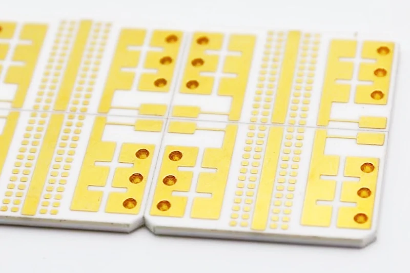
Thick Film Ceramic PCBs are created by applying a thick layer of conductive material (usually gold paste) on a ceramic substrate, followed by baking at temperatures below 1000°C. This process is ideal for large-scale production, especially in industries that require high-volume manufacturing. However, the cost of gold limits its use in some applications.
Applications:Common in consumer electronics, automotive applications, and power supplies where high-volume production is needed.
Key Features:
- Ideal for mass production
- Limited by the high cost of gold
- Multi-layer copper circuit options are available
Ceramic PCB vs. Aluminum PCB vs. FR4: A Comparison
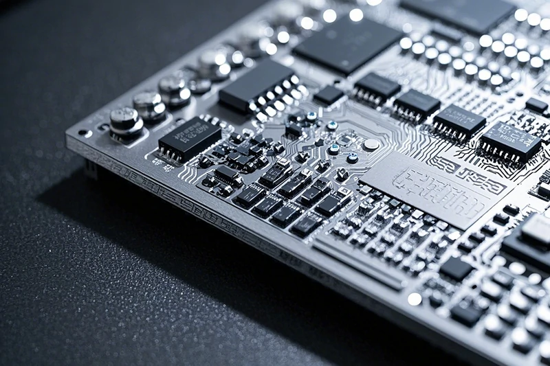
Ceramic PCBs are an ideal choice for applications requiring superior thermal conductivity, higher heat resistance, and excellent performance at high frequencies. These boards are commonly used in demanding industries such as aerospace, medical, and high-power electronics. Ceramic materials also offer excellent electrical insulation, which makes them suitable for use in harsh environments. Their ability to dissipate heat effectively helps in applications where thermal management is critical.
When comparing ceramic PCBs to aluminum PCBs, ceramic materials consistently outshine aluminum in terms of thermal conductivity. While aluminum can conduct heat at around 237 W/(m.k), ceramic materials such as aluminum nitride and beryllium oxide offer superior thermal management. Additionally, ceramic PCBs do not require an insulation layer like aluminum PCBs, which gives them a distinct edge in high-performance applications.
FR4 is the most widely used PCB material in electronics. It is a glass-reinforced epoxy laminate that offers a balance of strength, flexibility, and electrical insulation. FR4 PCBs are cost-effective, easy to manufacture, and versatile, making them suitable for a wide range of applications such as consumer electronics, communication devices, and power systems. However, they do not perform as well as ceramics in high-temperature or high-frequency environments.
Advantages of Mars PCB Manufacturing
At Mars PCB, we utilize 99.96% aluminum nitride and aluminum oxide, combined with high-performance metal layers that provide low resistance and strong adhesion, ensuring the durability and efficiency of our ceramic PCBs.
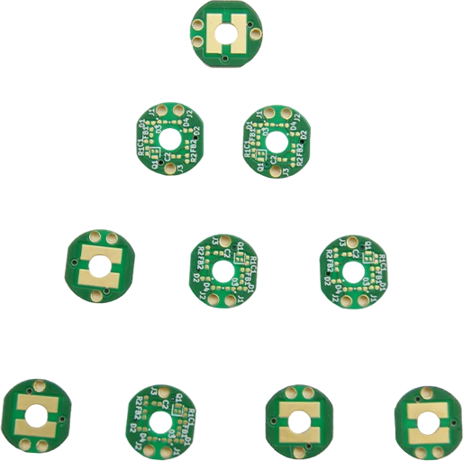
Mars PCB is equipped with state-of-the-art machinery, including laser depaneling for round ceramic PCBs and diamond-cutting for rectangular designs, to ensure precision and quality at every step.
Our skilled professionals use advanced DPC (Direct Plating Copper) technology to produce high-performance, customizable ceramic PCBs. We also offer HTCC, DBC, LTCC, and thin-film options.
Mars PCB manufactures ceramic PCBs without an oxide layer, ensuring longevity and high reliability, even in challenging environments.
We offer full flexibility in copper thickness customization, ranging from 1μm to 1mm. Our HDI capability enables us to create smaller, lighter, and thinner products, tailored to your specific needs.
Mars PCB provides a variety of shipping options including air, sea, and rail through trusted carriers like DHL, FedEx, and UPS, giving you flexibility in choosing your preferred delivery method.
Ceramic PCB Manufacturing Process
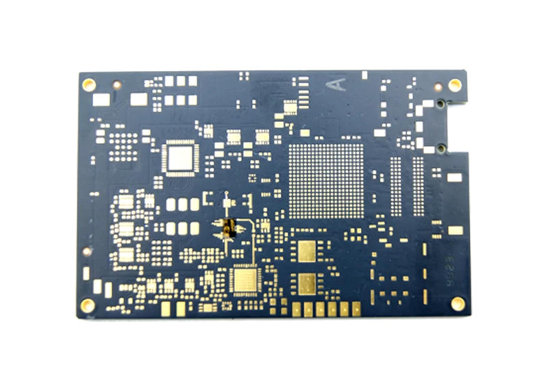
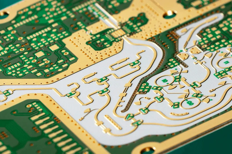
Ceramic PCBs consist of a ceramic substrate with copper layers applied through methods such as sputtering, plating, sintering, or brazing. Depending on the ceramic material, we manufacture AlN PCBs, alumina PCBs, SiC PCBs, Si₃N₄ PCBs, BeO PCBs, and hybrid ceramic PCBs.
Ceramic PCB manufacturing processes include LTCC, HTCC, DPC, DBC, thick-film, thin-film, and AMB.
We use two main lamination techniques:
- Normal Lamination: In this process, two ceramic layers are bonded with a dielectric layer (PP). While it is cost-effective, it reduces thermal conductivity compared to sintering lamination.
- Sintering Lamination: This process integrates the two ceramic layers under high pressure and temperature, providing superior thermal conductivity, high reliability, and improved bonding strength.
Direct Plating Copper (DPC) for Ceramic PCB Manufacturing
DPC is an advanced processing method at Mars PCB. Developed from thin-film technology, DPC allows us to achieve micron-level precision for ceramic PCB production without any restrictions on ceramic type or thickness.
The DPC process involves:
- Cleaning the ceramic substrate.
- Sputtering a copper composite layer onto the ceramic surface.
- Exposing and developing the photoresist layer for circuit patterning.
- Electroplating to increase copper thickness.
- Removing the photoresist, leaving a finished circuit.
DPC is faster and more precise than traditional thick-film and thin-film methods, enabling us to meet high-demand projects with excellent quality.
Ceramic PCB Depaneling at Mars PCB
Depaneling is the process of separating individual ceramic PCBs from a production panel. At Mars PCB, we use laser-cutting for round PCBs and diamond-cutting for rectangular ones, ensuring clean edges and preventing damage to the circuits.
Laser depaneling for round ceramic PCBs uses nitrogen to lower temperatures and prevent circuit damage, while diamond depaneling is ideal for rectangular shapes, providing precise cuts without risk of carbonization.
Ceramic PCB Manufacturing Capabilities
Specification | Mars PCB Ceramic PCB Capabilities |
PCB Layer Quantity | 1, 2 (single-sided and double-sided) |
Lead Time | 1 day to 4 weeks |
Ceramic Materials | AlN, Al₂O₃, SiC, BeO, Si₃N₄, Rogers |
Manufacturing Methods | DPC, DBC, HTCC, LTCC, thick-film, thin-film, AMB |
Max PCB Size | 138mm x 190mm |
PCB Thickness | 0.25mm to 2mm |
Trace Width/Space | 5-10μm: 0.05mm/0.05mm, 1OZ: 0.1mm/0.1mm |
Copper Thickness | 2μm to 105μm (DPC), 150μm to 300μm (DBC) |
Laser Drilling | ≥75μm |
Solderability | >95% |
Surface Finish | OSP, immersion silver, immersion gold, nickel-palladium gold |
Challenges in Ceramic PCB Manufacturing and Solutions
While ceramic PCBs offer numerous benefits, their manufacturing process presents some challenges. Here are the common challenges faced during the production of ceramic PCBs and the solutions to address them

Challenge: Material Brittleness
Ceramic materials are naturally more brittle than FR4 and can crack or break during handling or processing.
Solution: Manufacturers use precision machinery and controlled environments during handling and assembly to minimize stress on ceramic materials. Additionally, specialized techniques such as laser cutting and advanced molding processes are used to ensure precise cutting and shaping.

Challenge: High Production Costs
Ceramic PCBs are more expensive to produce than traditional FR4 PCBs due to the specialized materials and advanced manufacturing techniques involved.
Solution: To mitigate cost issues, manufacturers can focus on optimizing production workflows, reducing material waste, and investing in automation to streamline the production process.

Challenge: Complex Design Requirements
Designing ceramic PCBs requires advanced skills and tools, as the material has different thermal and electrical properties compared to conventional materials.
Solution: Close collaboration between designers and manufacturers ensures the PCB is designed to meet both the electrical and thermal requirements. Using advanced simulation software also helps identify potential design flaws early on in the process.

Challenge: Limited Flexibility
Ceramic PCBs are rigid, which may not be suitable for designs requiring flexible materials.
Solution: For applications needing flexibility, manufacturers may offer a hybrid solution, using flexible materials for specific parts of the design while incorporating ceramic for areas requiring high heat resistance.

Challenge: Heat Management in High-Power Applications
Managing heat dissipation is crucial in high-power applications, and while ceramic PCBs excel in this area, ensuring consistent thermal performance can still be challenging.
Solution: Advanced thermal simulation techniques and improved cooling solutions, such as heat sinks and active cooling methods, are incorporated into the design to optimize heat management.
Applications of Ceramic PCBs
Ceramic PCBs are highly suitable for a variety of high-performance applications where traditional materials may not suffice. Here are some key industries and applications that benefit from ceramic PCBs.
Memory Modules
Ceramic PCBs offer high thermal conductivity and insulation, making them ideal for memory modules in electronic devices that require consistent cooling and high-frequency performance.
Transmission Modules
In high-speed communication devices, ceramic PCBs enable efficient signal transmission due to their low signal loss and high-frequency stability.
Multilayer Interconnect Boards
For advanced electronics that require multi-layer interconnects, ceramic PCBs ensure optimal heat dissipation and signal integrity across layers.
Analog/Digital PCBs
Ceramic PCBs are ideal for mixed-signal applications, providing reliable operation for both analog and digital circuits.
High Power LED
Ceramic PCBs are widely used in high-power LED applications due to their exceptional heat dissipation properties, which help prevent overheating and extend the lifespan of the LEDs.
Solar Panels
Ceramic PCBs are used in solar panel systems, where they help manage high thermal loads while ensuring long-term durability in outdoor environments.
Electrical Power Transmitters
Ceramic materials support efficient power transmission, making them a preferred choice for power inverters and converters in various electrical systems.
Semiconductor Coolers
The high thermal conductivity of ceramic PCBs makes them perfect for semiconductor cooling, ensuring optimal temperature management in electronic devices.
Professional PCB & PCB Assembly Manufacturer & Factory
From concept to completion, your project will be under experienced project management, sparing you the hassle of untimely conference calls, communication gaps, language barriers and “real time” information gathering.