
The primary reason multilayer PCBs are significantly more expensive than single-layer PCBs is the increased material cost and complex manufacturing processes, including multiple lamination cycles, precise drilling, and intricate plating required to connect the inner layers. While a single-layer board involves a straightforward process of etching a single copper sheet, a multilayer board is a sophisticated sandwich of materials and circuitry, where each additional step introduces more time, specialized equipment, and a higher risk of defects, all of which directly drive up the final cost.
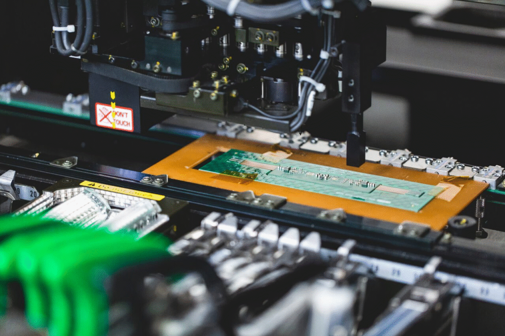
Table of Contents
- What Are Single-Layer and Multilayer PCBs? A Quick Primer
- The Core Question: Why is There Such a Significant Cost Difference?
- A Deep Dive into the Primary Cost Drivers
- Detailed Cost Breakdown: Single-Layer vs. Multilayer PCBs
- When Does a Multilayer PCB Become the More “Cost-Effective” Choice?
- Practical Tips for Optimizing Your PCB Manufacturing Costs
- Conclusion: Making an Informed Decision for Your Project
- Frequently Asked Questions (FAQ)
Multilayer vs. Single-Layer PCB: A Comprehensive Cost Analysis
When developing an electronic product, one of the most fundamental design decisions revolves around the Printed Circuit Board (PCB). The choice between a simple single-layer PCB and a more complex multilayer PCB has profound implications not just for the device’s functionality and size, but also for its manufacturing cost. Understanding the cost drivers behind each option is crucial for engineers, project managers, and businesses aiming to balance performance with budget. This article provides an in-depth comparison of the manufacturing costs, exploring exactly where the expenses originate and how to make the most cost-effective decision for your specific application.
What Are Single-Layer and Multilayer PCBs? A Quick Primer
Before dissecting the costs, it’s essential to understand the fundamental structural differences between these two types of circuit boards. Their construction is the very foundation of their cost disparity.
A Single-Layer PCB, also known as a single-sided board, is the most basic type of circuit board. It consists of a single layer of conductive material (typically copper) on one side of a non-conductive substrate, such as FR-4 fiberglass. Components are mounted on one side, and the entire circuit is etched on the other. Due to their simplicity, they are ideal for low-density designs like power supplies, relays, and simple sensor circuits where complexity is minimal.
A Multilayer PCB, by contrast, is composed of three or more conductive copper layers laminated together with insulating material. These boards are created by bonding alternating layers of prepreg (a fiberglass cloth pre-impregnated with epoxy resin) and core materials. The inner layers allow for much denser and more complex routing of traces, making them indispensable for sophisticated electronics like smartphones, computers, and medical equipment. Vias—small drilled holes—are used to create electrical connections between the different layers.
The Core Question: Why is There Such a Significant Cost Difference?
The journey from a digital design file to a physical PCB is vastly different for single-layer versus multilayer boards. The cost premium for multilayer PCBs isn’t arbitrary; it’s a direct reflection of the additional materials, intricate manufacturing steps, increased labor, and higher quality control standards required. Each additional layer doesn’t just add a sheet of copper; it adds a full cycle of imaging, etching, inspection, and lamination, exponentially increasing the complexity and potential for error. This cumulative process is the primary reason a four-layer board can cost several times more than a single-layer board of the same dimensions.
A Deep Dive into the Primary Cost Drivers
To truly grasp the price difference, we must break down the manufacturing process into its core cost components. Four key areas contribute most to the final price: materials, process complexity, labor and yield, and testing.
Cost Driver 1: Raw Materials and Composition
The bill of materials for a PCB goes beyond the basic substrate. For a single-layer board, the material list is short: one layer of copper foil bonded to a substrate like FR-4. It’s a simple, mass-produced material with a relatively low cost.
For a multilayer PCB, the material requirements escalate quickly. In addition to the standard copper-clad cores, manufacturers must use multiple sheets of prepreg. This is a crucial insulating material that acts as the “glue” to bond the layers together during the lamination process. Each layer pair requires its own sheet of prepreg. Therefore, a 6-layer board requires significantly more copper foil, prepreg, and core material than a single-layer or even a 2-layer board. This direct increase in raw material quantity is a foundational element of the higher cost.
Cost Driver 2: Manufacturing Process Complexity
This is arguably the most significant cost driver. The manufacturing workflow for a multilayer PCB is an order of magnitude more complex than for a single-layer board. A single-layer board undergoes a simple process: drill, image, etch, and apply a solder mask. It’s a linear and relatively quick procedure.
A multilayer board, however, requires a multi-stage, iterative process. Each inner layer must be individually imaged and etched before being stacked. The stack is then put through a lamination cycle, which involves applying intense heat and pressure to bond the layers and prepreg together into a single, solid board. After lamination, the board must be drilled. This drilling is more complex, as it includes creating vias to connect different layers. Specialized vias like blind vias (connecting an outer layer to an inner layer) and buried vias (connecting two inner layers) add even more steps and require advanced machinery, further inflating the cost. Each of these additional steps—layer alignment, lamination, and complex drilling—requires precise calibration and specialized equipment, contributing heavily to the final price.
Cost Driver 3: Labor, Time, and Yield Rates
More process steps naturally translate to more labor hours and longer production times. Aligning multiple layers with micron-level precision, operating lamination presses, and running complex drilling programs all require skilled technicians and more machine time. This extended time on the production floor is a direct cost.
Furthermore, complexity increases the probability of manufacturing defects. With a single-layer board, the potential for error is low. With a multilayer board, a single mistake on an inner layer—such as a misaligned trace or a short circuit—can render the entire board useless, as it’s impossible to fix once the layers are laminated. This reality leads to lower yield rates (the percentage of usable boards from a production panel). Manufacturers must factor this potential for scrap into their pricing, meaning you pay not only for the successful boards but also for the risk associated with producing them.
Cost Driver 4: Design and Testing Requirements
The intricate nature of multilayer PCBs necessitates more rigorous inspection and testing. While a single-layer board can be quickly inspected visually or with a simple electrical test, multilayer boards require more sophisticated methods. Automated Optical Inspection (AOI) is used to check each inner layer before lamination. After assembly, X-ray inspection may be needed to verify the alignment of inner layers and the integrity of vias.
Electrical testing is also more complex. A “bed of nails” or flying probe tester must verify connectivity not just across a single surface, but between all layers of the board. This comprehensive testing adds time and requires expensive equipment, further contributing to the overall manufacturing cost.
Detailed Cost Breakdown: Single-Layer vs. Multilayer PCBs
To visualize the differences, here is a comparative table highlighting the key cost factors for a standard-sized board.
| Cost Factor | Single-Layer PCB | Multilayer PCB (e.g., 4-Layer) |
|---|---|---|
| Raw Materials | Low (1x FR-4 Core, 1x Copper Foil) | High (1x Core, 2x Copper Foil, 2x Prepreg) |
| Lamination Process | Not required. | Required; a critical, time-consuming step. |
| Drilling Complexity | Simple through-holes. | Complex; requires precise vias (through, blind, buried). |
| Imaging & Etching | One cycle for the single copper layer. | Multiple cycles (one for each layer). |
| Production Time | Short. | Significantly longer due to multiple process cycles. |
| Typical Yield Rate | Very High (>98%). | Lower; decreases as layer count increases. |
| Testing & Inspection | Basic electrical and visual inspection. | Advanced AOI for inner layers and complex electrical testing. |
When Does a Multilayer PCB Become the More “Cost-Effective” Choice?
While multilayer PCBs have a higher per-unit manufacturing cost, they can sometimes be the more economical choice when considering the project as a whole. The decision transcends the simple price tag of the board itself.
Addressing Miniaturization and Space Constraints
If your product design demands a small form factor, trying to cram a complex circuit onto a large single-layer board might be impossible or require a much larger and more expensive enclosure. A compact 4-layer board allows for much denser component placement and routing, enabling a smaller overall product. In this scenario, the higher cost of the PCB is offset by savings on the enclosure and the increased marketability of a smaller, sleeker device.
Meeting High-Frequency and Signal Integrity Demands
For high-speed digital circuits or sensitive analog applications, signal integrity is paramount. Multilayer boards offer significant advantages here. They allow designers to create dedicated ground and power planes, which provide excellent shielding against electromagnetic interference (EMI) and reduce noise. This controlled impedance environment is crucial for the reliable operation of high-frequency signals. Achieving similar performance on a single-layer board would be extremely difficult and might require costly external shielding or filtering components, ultimately driving the total system cost up.
Considering the Total Cost of Ownership (TCO)
The total cost of ownership includes not just the manufacturing cost but also design time, assembly, testing, and potential failure rates in the field. A well-designed multilayer board can be more reliable and easier to assemble than a sprawling, complex single-layer design. The improved performance and reliability can lead to lower warranty claims and a better customer experience, which are invaluable long-term benefits. Therefore, while the initial outlay is higher, the TCO of a multilayer solution can sometimes be lower.
Practical Tips for Optimizing Your PCB Manufacturing Costs
Regardless of your choice, there are always ways to manage costs:
- Stick to Standard Layer Counts: A 4-layer or 6-layer board is far more standard (and thus cheaper) to produce than a 3-layer or 5-layer board, which requires an unconventional manufacturing process.
- Optimize Board Size: Manufacturers often price based on how many boards they can fit on a standard production panel. Work with your fabricator to find an optimal board dimension that minimizes waste.
- Avoid Exotic Vias: Standard through-hole vias are the cheapest. Blind and buried vias add significant cost due to extra lamination and drilling steps. Use them only when absolutely necessary.
- Minimize Trace/Space Width: The smaller your trace and space requirements, the higher the precision needed, and the higher the cost. Stick to the manufacturer’s standard capabilities unless your design demands otherwise.
Conclusion: Making an Informed Decision for Your Project
The cost difference between single-layer and multilayer PCBs is not a simple markup but a direct result of tangible factors: more materials, more complex and time-consuming processes, and more rigorous quality control. A single-layer PCB is the undisputed champion of low cost for simple, low-density electronics. However, for complex, compact, or high-performance devices, a multilayer PCB is an essential investment. The key is to evaluate the needs of your entire project. By understanding the cost drivers detailed above, you can make an informed, strategic decision that balances the per-unit price of the board with the overall performance, size, and reliability requirements of your final product.
Frequently Asked Questions (FAQ)
1. How much more expensive is a 4-layer PCB than a 2-layer PCB?
As a general rule of thumb, a 4-layer PCB can be 40% to 60% more expensive than a 2-layer PCB of the same dimensions and specifications. This is because moving from 2 layers to 4 introduces the need for inner layer imaging, prepreg materials, and a full lamination cycle, which are not required for a standard 2-layer board.
2. Is a single-layer PCB ever a better choice for high-volume production?
Absolutely. If the circuit is simple enough to fit comfortably on a single layer, its low manufacturing cost makes it the ideal choice for high-volume, cost-sensitive products like toys, simple calculators, or LED lighting controllers. The cost savings per board, multiplied over millions of units, are substantial.
3. Do material choices like FR-4 affect the cost difference?
While the type of substrate material (e.g., standard FR-4 vs. high-frequency Rogers material) affects the absolute cost of any PCB, it doesn’t fundamentally change the relative cost difference. A multilayer board will always be more expensive than a single-layer board made from the same material due to the additional process steps and quantities of that material required.
Multilayer PCBs vs Single-Layer PCBs, PCB manufacturing cost, single-layer pcb cost, multilayer pcb price, cost factors for pcb fabrication, what makes multilayer pcbs expensive, printed circuit board cost comparison, 2-layer vs 4-layer pcb cost, how to reduce pcb manufacturing costs, choosing between single and multilayer pcb

