In the modern landscape of electronics design, the distinction between “working” and “failing” is no longer defined merely by logical connectivity. As data rates accelerate beyond Gigabit speeds and rise times shrink into the picosecond domain, the physical layout of a Printed Circuit Board (PCB) transforms from a simple carrier of current into a complex network of high-frequency transmission lines.
For the Hardware Engineer and Signal Integrity (SI) Specialist, two primary adversaries exist in this domain: Signal Reflection and Crosstalk.
While both phenomena degrade signal quality, cause bit errors, and close eye diagrams, they originate from fundamentally different physical mechanisms. One is an issue of longitudinal continuity (Reflection), while the other is an issue of lateral proximity (Crosstalk). Confusing the two leads to ineffective debugging—adding a termination resistor will never fix crosstalk, and increasing trace spacing will never fix a reflection.
This comprehensive guide provides an in-depth engineering analysis of these two phenomena, detailing their physics, mathematical foundations, diagnostic “signatures” on an oscilloscope, and advanced mitigation strategies for 2025-era designs.

I. The Physics of the Transmission Line
To understand why these issues occur, we must first abandon the “lumped element” model of circuits (where wires are instant) and adopt the distributed element model.
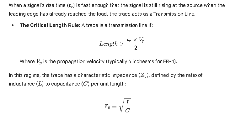
If the signal encounters any deviation from this $Z_0$ environment, or if it encounters the electromagnetic fields of a neighbor, the integrity of the waveform is compromised.
II. Signal Reflection: The Echo Chamber
Reflection is strictly a single-net phenomenon. It does not require a neighbor. It occurs when a traveling wave encounters an Impedance Discontinuity.
1. The Mechanics of Discontinuity
Imagine a beam of light hitting a glass window. Some light passes through (refraction), but some bounces back (reflection). The same physics applies to electrons.
When a signal traveling on a 50$\Omega$ trace hits a component pin, a via, or a connector with a different impedance (say, 30$\Omega$ capacitive load), the energy cannot simply vanish. To satisfy the boundary conditions of voltage and current conservation, a portion of the signal must reflect back toward the source.
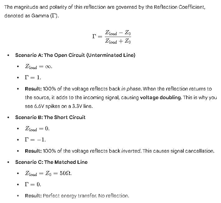
2. The Mathematics: Reflection Coefficient ($\Gamma$)
3. The Lattice Diagram (Bounce Diagram)
Reflections don’t happen just once. The reflected wave travels back to the source. If the source is also mismatched (e.g., a low-impedance driver), the wave reflects again back to the load.
This ping-pong effect creates Ringing.
- Featured Snippet: Ringing is the damped sinusoidal oscillation seen on a signal edge, caused by multiple reflections bouncing back and forth between mismatched source and load impedances. It persists until resistive losses in the trace dissipate the energy.
4. Visual Symptoms of Reflection
How do you identify reflection on an oscilloscope?
- Overshoot/Undershoot: Massive spikes immediately following a transition.
- Stair-stepping (The Plateau): On long traces, the signal rises to half amplitude, stays flat for the round-trip time ($2 \times T_{flight}$), and then jumps to full amplitude. This is a classic signature of a series-terminated line measuring at the driver.
- Non-Monotonic Edges: The voltage rises, dips back down, and rises again. This can cause double-clocking in flip-flops.
III. Crosstalk: The Electromagnetic Intruder
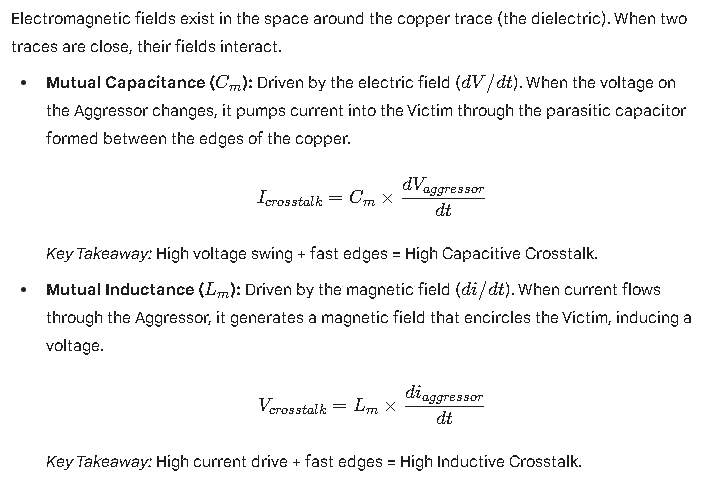
Crosstalk is a multi-net phenomenon. It is the unintentional coupling of electromagnetic energy from an “Aggressor” trace to a “Victim” trace. It is essentially a transformer created by PCB layout.
1. The Physics: Capacitive and Inductive Coupling
2. NEXT vs. FEXT: Direction Matters
Crosstalk propagates in two directions relative to the Aggressor’s signal.
- Near-End Crosstalk (NEXT):
Noise that travels backward toward the source.- Behavior: It appears immediately when the Aggressor switches. It is usually the dominant noise source in connectors and cable assemblies.
- Far-End Crosstalk (FEXT):
Noise that travels forward along with the signal to the receiver.- Behavior: It accumulates over the length of the run.
- The Stripline Advantage: In a stripline environment (inner layer trace sandwiched between two ground planes), the inductive and capacitive FEXT currents are nearly equal and opposite, effectively cancelling each other out. This is why critical high-speed signals are often routed on inner layers.
3. Visual Symptoms of Crosstalk
Crosstalk is often mistaken for random noise, but it is correlated to the aggressor’s activity.
- Jitter: If the Aggressor switches at the same time the Victim is switching, the crosstalk alters the flight time of the Victim’s signal. This pushes the edge early or late, collapsing the horizontal eye opening.
- Logic Glitches: A static “Low” signal suddenly spikes high enough to cross the $V_{IH}$ threshold, causing a false bit.
- Vertical Eye Closure: The noise rides on top of the High and Low levels, reducing the voltage margin.
IV. Diagnostic Guide: Sherlock Holmes of the PCB
When a board fails, you rarely get an error message saying “Crosstalk Error.” You get a Bit Error Rate (BER) or a system crash. Here is how to distinguish the two culprits in the lab.
Test 1: The “Quiet Line” Analysis
- Keep the Victim line held Low (logic 0) or High (logic 1).
- Aggressively switch the neighboring data lines (stress test pattern).
- Measure the “Quiet” Victim line.
- Result: If you see spikes that coincide with the neighbor’s clock, It is Crosstalk. Reflection cannot exist on a line that isn’t switching (mostly).
Test 2: The TDR (Time Domain Reflectometry) Sweep
A TDR instrument (or a high-end scope with TDR module) sends a step pulse down the line and listens for echoes.
- Reflection Signature: The TDR plot shows “mountains and valleys.” A dip means low impedance (capacitive discontinuity); a peak means high impedance (inductive discontinuity). This confirms impedance mismatch.
- Crosstalk Signature: If the TDR line is perfectly flat (50$\Omega$) but the signal is still bad, the issue is external (Crosstalk) or loss-related.
Test 3: The S-Parameter Check (Frequency Domain)
If you have a Vector Network Analyzer (VNA), look at the S-Parameters.
- $S_{11}$ (Return Loss): Measures energy reflecting back. High $S_{11}$ (e.g., -5dB) indicates severe Reflection issues.
- $S_{21}$ (Insertion Loss): Measures energy getting through.
- $S_{41}$ (Far End Crosstalk): Measures energy transferring from Port 1 to Port 4. High values here confirm Crosstalk.
V. Mitigation Strategies for Reflection
To fix reflection, you must manage Impedance. You cannot “shield” against reflection; you must “absorb” it.
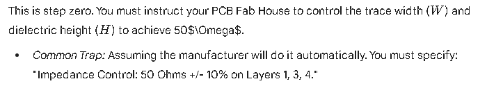
1. Controlled Impedance Fabrication
2. Termination Techniques
Termination adds resistance to match the line impedance, absorbing the energy so it doesn’t bounce.
- Series Termination (Source Termination):
- Method: A resistor ($R_s$) is placed in series with the output pin. $R_{driver} + R_s = Z_0$.
- Use Case: Point-to-point topologies (e.g., SPI, clock signals).
- Advantage: Consumes zero DC power.
- Parallel Termination (Load Termination):
- Method: A resistor ($R_p$) connects the signal line to Ground (or Vtt) at the receiver end.
- Use Case: High-speed busses (DDR) and multi-drop buses.
- Disadvantage: Burns continuous DC power.
- Thevenin Termination:
- Method: A pull-up and pull-down resistor pair.
- Use Case: Legacy busses requiring specific voltage levels.
- ODT (On-Die Termination): Modern chips (DDR4/5, PCIe) have selectable resistors built into the silicon. Always check your register settings to ensure ODT is enabled.
3. Via Management (Back-drilling)
At 25 Gbps+, a standard Via Stub (the unused part of the plated hole) acts as an open-circuited transmission line stub. It creates a notch filter, reflecting specific frequencies.
- Solution: Back-drilling. The fab house drills out the unused copper barrel from the bottom side, minimizing the stub length.
VI. Mitigation Strategies for Crosstalk
To fix crosstalk, you must manage Geometry and Fields.
1. The 3W Rule (and 10W Rule)
The most effective fix is distance. The electromagnetic field strength decays with the square of the distance ($1/d^2$).
- The Rule: Keep the center-to-center spacing of traces at least 3x the trace width. This reduces crosstalk flux by approx 70%.
- The Aggressive Rule: For clock lines or sensitive analog traces, use 10W spacing.
2. Differential Signaling
Why do USB, PCIe, and Ethernet use differential pairs? Common Mode Rejection.
- If crosstalk hits a differential pair (D+ and D-), it tends to induce the same noise voltage on both lines.
- The receiver looks at the difference ($V_{diff} = D+ – D-$).
- $(D+ + Noise) – (D- + Noise) = D+ – D-$. The noise cancels out.
- Note: This only works if the traces are tightly coupled to each other but loosely coupled to aggressors.
3. Reference Plane Management (The Return Path)
Crosstalk is essentially “Return Path Contention.”
- If two traces share a narrow return path in the ground plane, the return currents interact.
- Solution: Solid Ground Planes. Never route high-speed signals over a split plane or a void.
4. Guard Traces (Use with Caution)
Some designers place a grounded trace between two signal traces to act as a shield.
- The Risk: If the guard trace is not stitched to the ground plane with vias at regular intervals (every $\lambda/10$), it becomes a resonant antenna and can actually increase crosstalk or radiate EMI. Use the 3W rule instead unless you are expert at guard trace stitching.
VII. Advanced Scenario: The DDR Memory Interface
Let’s apply this to a real-world example: DDR4/DDR5 Design.
- Reflection Challenge: The Address/Command bus is a “Fly-by” topology, hitting multiple memory chips in a chain. This creates complex reflections at every node.
- Fix: VTT termination at the very end of the bus and ODT on the DRAM chips.
- Crosstalk Challenge: The Data (DQ) lines are packed extremely tight to fit under the CPU.
- Fix: “Byte Lane Spacing.” Route DQ0-DQ7 tightly, but leave a larger gap before DQ8-DQ15.
- Fix: Alternating Layers. Route Byte 0 on Layer 3 and Byte 1 on Layer 5 (Stripline) to prevent broadside coupling.
VIII. Summary Comparison Matrix
For a quick reference during design reviews, use this comparison table.
| Feature | Signal Reflection | Crosstalk |
| Primary Cause | Impedance Mismatch ($Z_0 \neq Z_L$). | Mutual Capacitance ($C_m$) & Inductance ($L_m$). |
| Dependency | Single Trace (Self-inflicted). | Adjacent Traces (Neighbor-inflicted). |
| Timing Signature | Synchronous (Fixed delay from own edge). | Asynchronous (Correlated to neighbor). |
| Visual Signature | Overshoot, Undershoot, Ringing, Stair-step. | Jitter, Glitches, Eye Closure (Vertical). |
| Governing Math | Reflection Coefficient ($\Gamma$). | Coupling Coefficient ($k$). |
| Primary Mitigation | Termination ($R_s, R_{term}$), Back-drilling. | Spacing (3W Rule), Shielding, Differential Pairs. |
| Layer Preference | Indifferent (requires impedance control). | Stripline (Inner layers) preferred for FEXT cancellation. |
IX. Conclusion
In the high-stakes world of high-speed PCB design, hope is not a strategy. You cannot simply route connections and hope the signal arrives intact.
Reflection is managed by rigorous Impedance Control and precise Termination strategies. It requires you to treat the trace as a component, matching the driver to the line and the line to the load.
Crosstalk is managed by disciplined Layout Geometry. It requires you to respect the “personal space” of signals, utilizing the 3W rule and solid reference planes to confine electromagnetic fields.
By understanding the distinct physics of these two phenomena—the echo of Reflection and the interference of Crosstalk—you can interpret the chaotic squiggles on your oscilloscope, pinpoint the root cause, and implement the co0rrect solution. In the GHz era, this diagnostic capability is what separates a Board Designer from a Signal Integrity Engineer.

