Custom PCBs Assembly
Mars PCB specializes in Printed Circuit Board Assembly (PCBA), a vital service that ensures the functionality and reliability of all electronic devices. This process involves placing various components onto the PCB, essential for everything from smartphones to basic calculators. With our expert assembly techniques, Mars PCB ensures each PCB operates efficiently, supporting the complex designs and advanced features of today’s electronic products.
PCB manufacturers like Mars PCB are essential in creating the boards found in every device we use. From smartphones to simple gadgets, their performance relies on high-quality PCBs.
PCB vs. PCBA – What’s the Difference?
Have you ever opened your smartphone to see what’s inside? You’ll find components like the digitizer, battery, soldering, and, of course, the PCB. The logic board is the heart of your device, and any damage to it can render your device inoperative.
For example, the compact design of modern smartphones showcases advanced PCB engineering that few companies can match.
What Makes PCBs Unique?
What differentiates one PCB from another? What are the essential components of a PCB? Don’t worry!
We’ve prepared this guide to help you understand the materials used in PCBs and how manufacturers create them. Let’s start by exploring what PCBs are made of, followed by the manufacturing process, and finally, how to choose the right vendor for your needs.
What are PCBs?
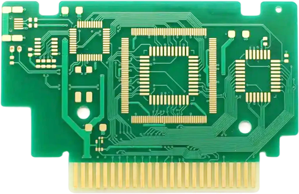
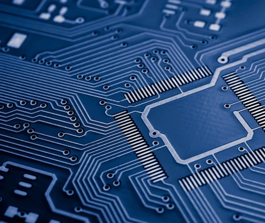
PCBs, or Printed Circuit Boards, are the foundational components of various electronic and electrical devices we use every day. Most PCBs consist of two or more layers, depending on the complexity and application of the device.
What Materials are Used in Printed Circuit Boards?
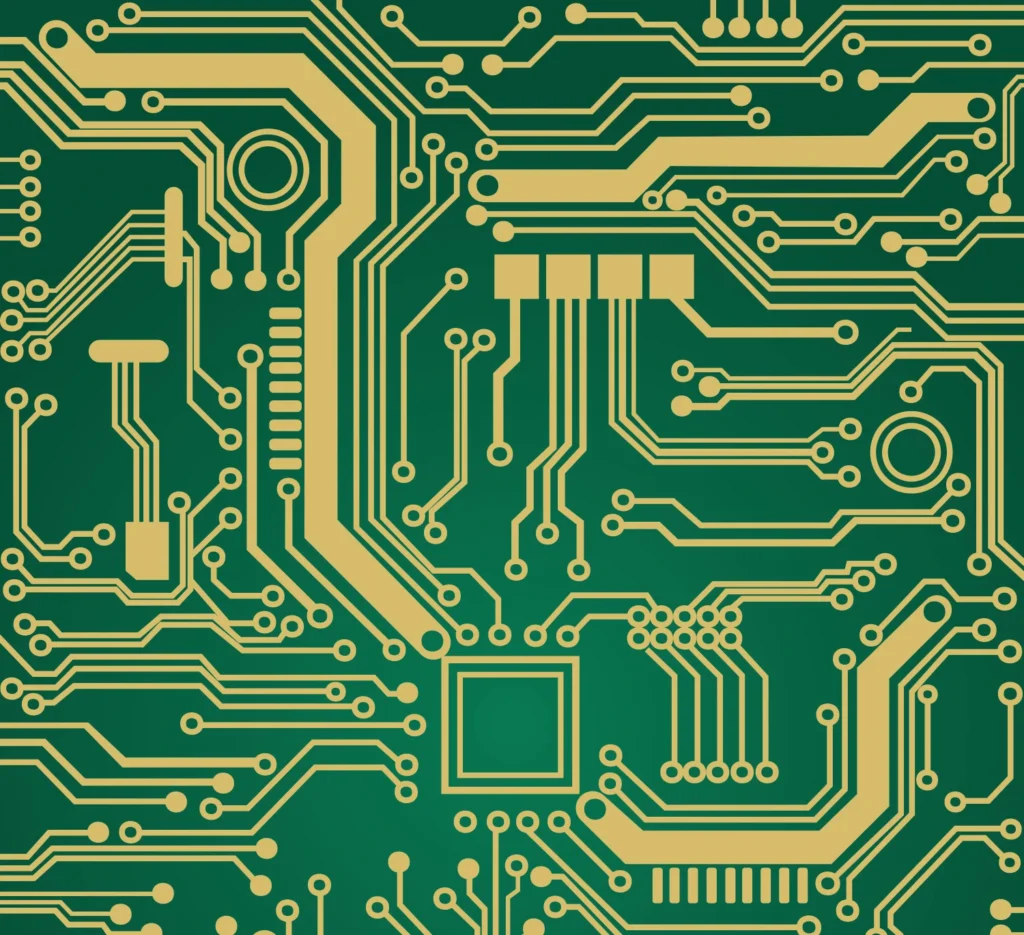
PCBs are made from a variety of materials. Layers can be composed of fiberglass or resin-based paper, along with copper, solder mask, and silkscreen layers.
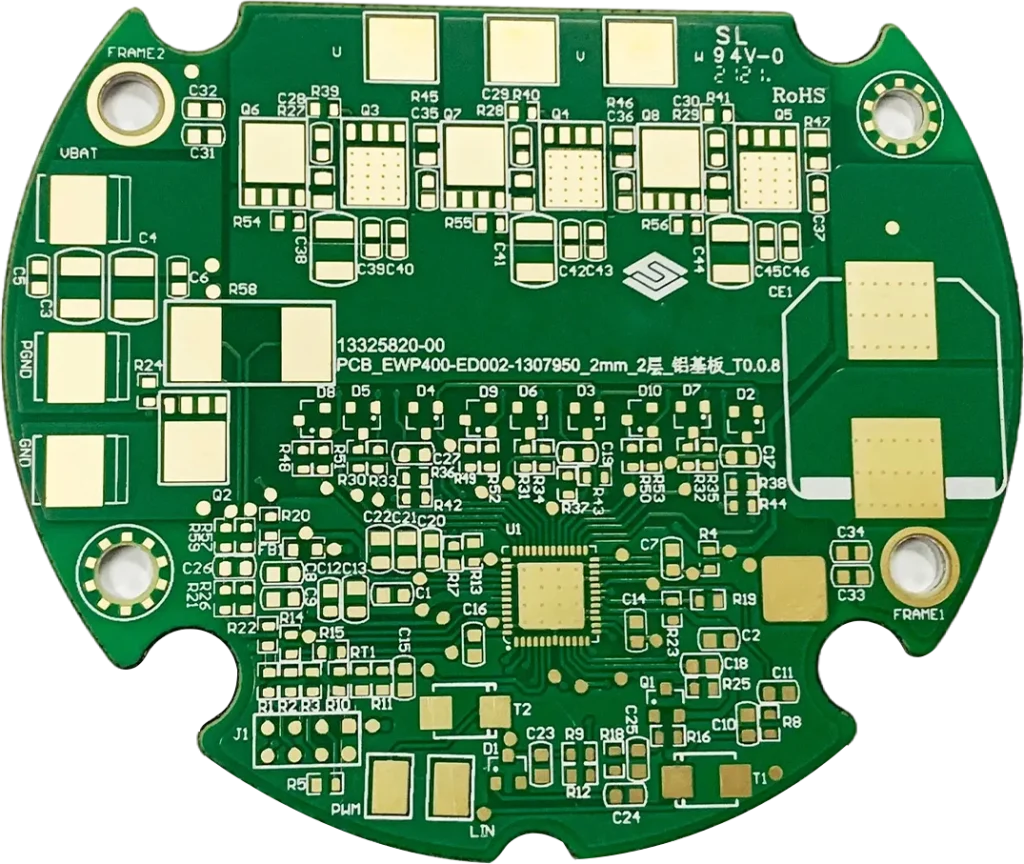
A typical PCB is made up of four layers bonded using heat and pressure. These layers include the substrate, copper, solder mask, and silkscreen.
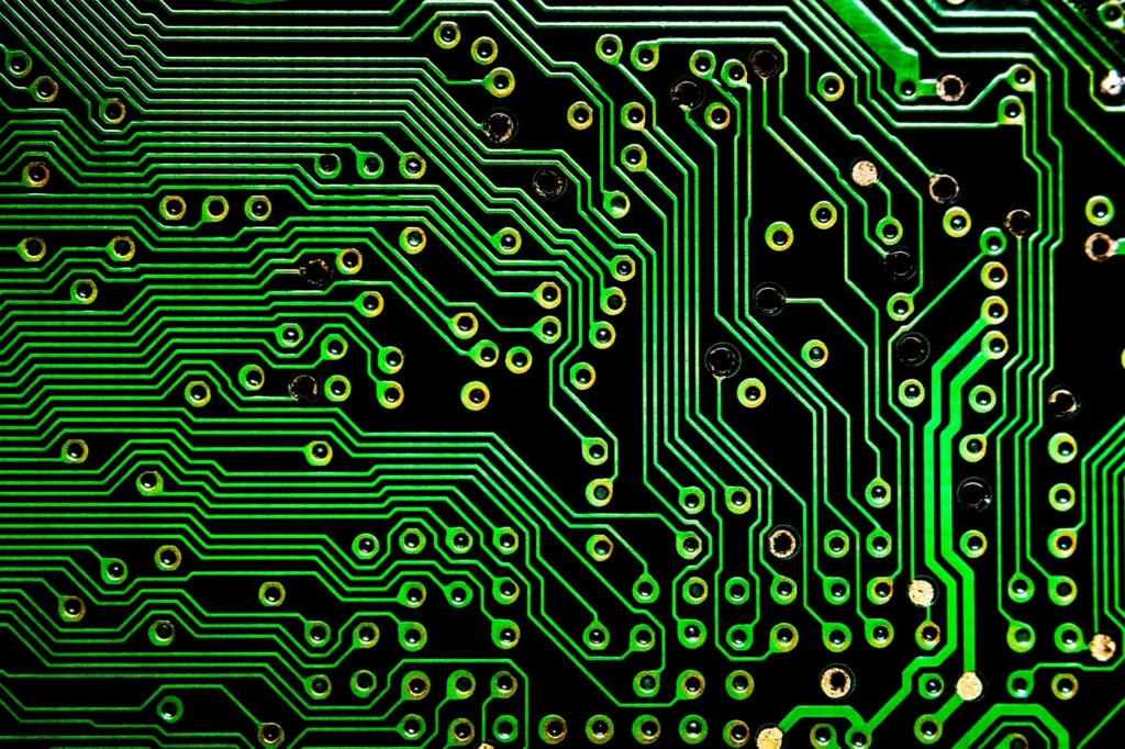
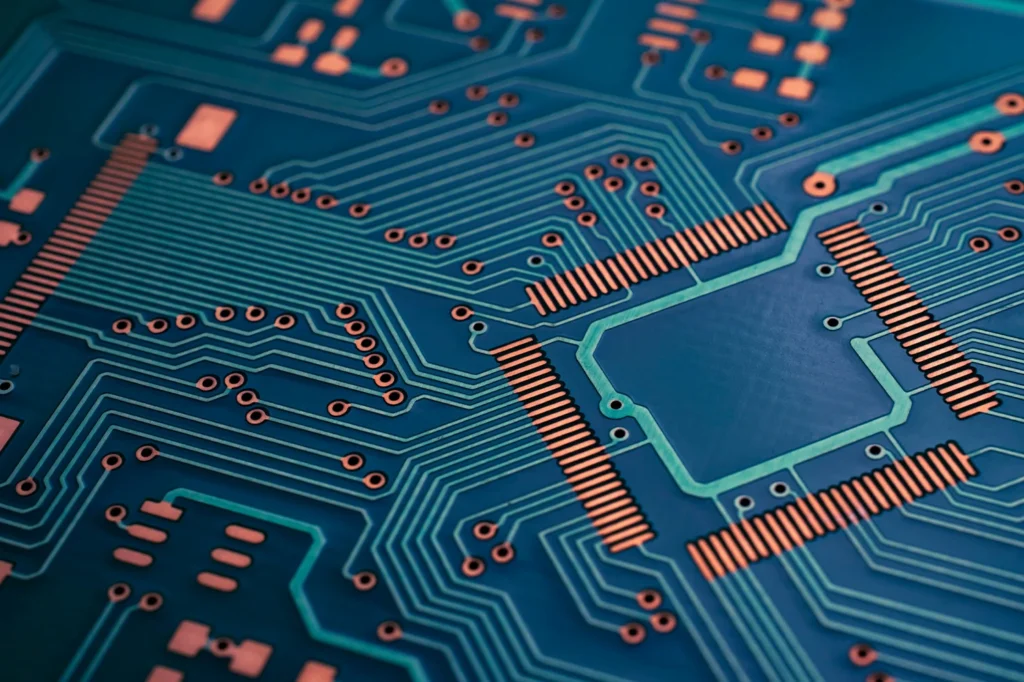
Copper is used as the primary conductive layer on the substrate. Depending on the PCB type and application, there can be one or two copper layers on either side of the substrate. Simple PCBs usually have a single copper layer, while more complex ones may have multiple layers to handle higher power and performance.
The silkscreen layer adds labels and indicators to the PCB, making it easier for engineers to identify components and connections.
The substrate, often made from FR4 (Fire Retardant 4), provides a sturdy base for the PCB. It ensures rigidity but can also be made flexible for certain applications. Advanced substrates may use innovative, eco-friendly materials.
The soldermask layer, typically green, protects the copper traces and prevents unwanted solder bridges. It ensures that electrical currents flow correctly within the PCB.
PCB Materials to Avoid
Not all PCB materials are suitable for every application. Some use epoxies, which can be thermally sensitive and prone to lamination loss. These cost-effective boards can be identified by their distinct smell during soldering and are not ideal for high-performance applications.
Types of PCB
PCBs are essential in various electronics, making daily tasks easier and more efficient.
Depending on the application, different types of PCBs are used to suit specific product needs.
Single-sided PCBs have one conductive layer. They are cost-effective and used in simple electronic devices. This type is ideal for basic manufacturing needs.
Double-sided PCBs have conductive layers on both sides of the substrate. They are more versatile and commonly used in more complex electronic devices, allowing for more components and connections.
Multilayer PCBs consist of multiple substrate and copper layers, providing higher performance and compact designs. They are used in advanced electronics like computers and smartphones.
Rigid PCBs are made from non-flexible materials like fiberglass, providing durability and stability for various applications.
Flex PCBs use flexible materials, allowing them to bend and fit into tight spaces. They are ideal for compact and wearable devices.
Rigid-Flex PCBs combine rigid and flexible materials, offering the benefits of both. They are used in complex and high-performance applications.
Custom PCB Components
Every electronic device requires specific components on its PCB to function correctly. Here are some essential components:
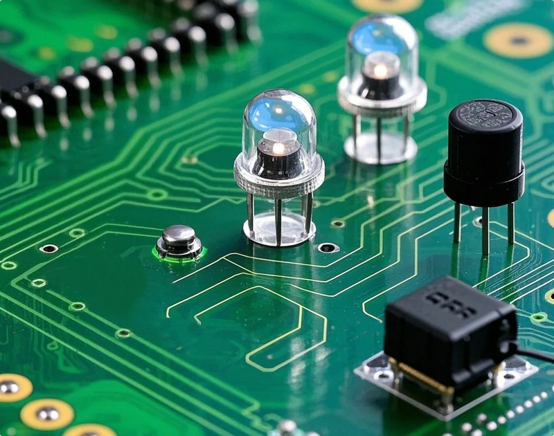
● LEDs: Light Emitting Diodes allow current to flow in one direction, providing indicators or lighting.
● Resistors: Control the flow of electrical current, ensuring proper functionality.
● Batteries: Supply power to the PCB, maintaining the device’s operation.
● Transistors: Amplify electrical signals, essential for processing information.
● Switches: Control the flow of electricity, allowing users to turn devices on or off.
● Buttons: Facilitate user interaction by controlling electrical pathways.
● Diodes: Allow current to flow in a single direction, protecting circuits from damage.
● Inductors: Store and release electrical energy, managing current flow.
Custom Made Circuit Boards
Designing a custom PCB can be challenging. Reliable software is essential for creating accurate blueprints. Tools like Eagle from Cadsoft Computer are excellent for designing PCBs.
Start by creating a schematic view in your design software. Add components from the library and connect their pins to represent electrical connections. Ensure all connections are accurate to avoid errors.
After finalizing the schematic, switch to the board layout view. Arrange components logically and route connections to create a functional PCB. Perform design checks to ensure there are no errors before manufacturing.
How Printed Circuit Boards are Made
Creating a PCB involves several stages, each requiring precision and advanced equipment. Here’s a brief overview of the manufacturing process.
The substrate forms the base of the PCB. It is prepared by spreading the material and applying epoxy resin. The substrate is then rolled to the desired thickness and cured in an oven to solidify.
Copper layers are added to the substrate to conduct electricity. Depending on the PCB's complexity, multiple copper layers may be used. Holes are drilled to connect different layers, and excess copper is removed to create the circuit pattern.
A solder mask is applied to protect the copper traces and prevent short circuits. It ensures that electrical currents flow correctly within the PCB. Labels and markings are added using silkscreen for easy identification of components.