HDI PCB Solutions: Engineering, Fabrication, and Next-Level Applications
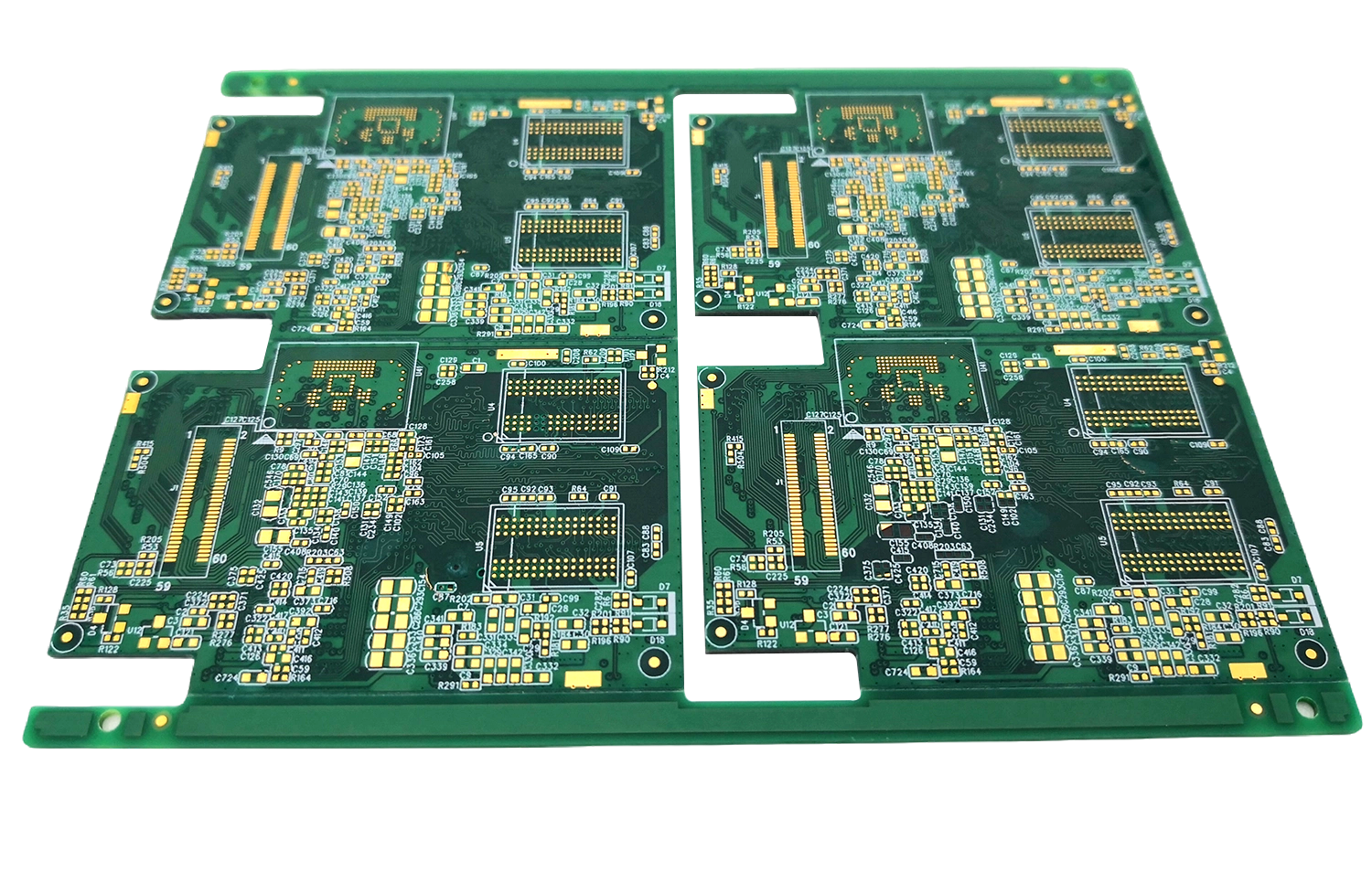
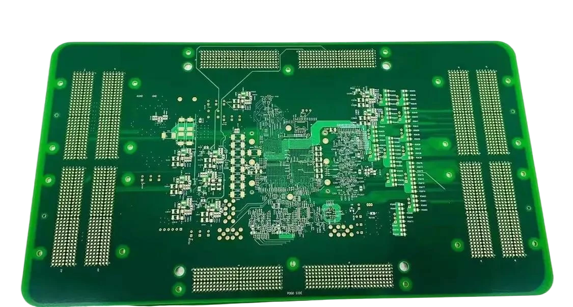
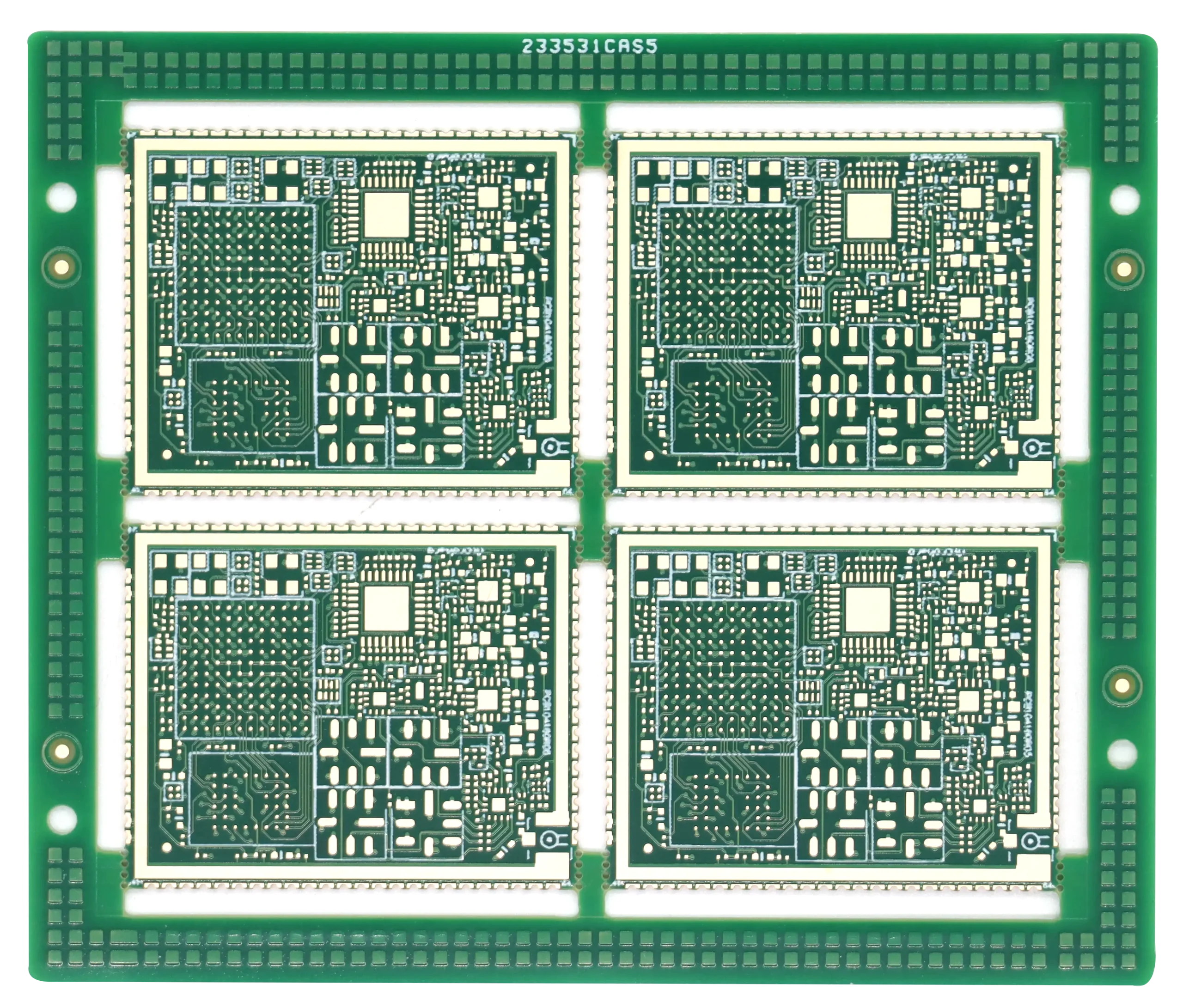
Mars PCB specializes in creating and assembling high-density interconnect (HDI) printed circuit boards. These advanced boards feature buried and blind via formations, microvia layers, and exceptional signal quality that support the most demanding electronic designs.
Defining HDI PCBs
High-Density Interconnect (HDI) PCBs stand out due to a greater concentration of traces per area, enabling more sophisticated circuitry in less space. What truly differentiates HDI PCBs from conventional boards is their focus on achieving finer line widths, denser via layouts, and multiple laminate build-up layers.
Hallmarks of HDI Boards
Several defining traits set these advanced boards apart:
Tight Trace/Space Dimensions
HDI circuitry features traces and spaces around or below 0.075 mm, markedly slimmer than the widths typical in traditional designs.
Reduced Via Size
Microvias, measuring under 150 microns in diameter, are fundamental for achieving greater density.
High Pad Density
An HDI design can exceed 200 component connection pads per square inch, fostering more compact assembly.
Expanded Layer Options
While standard PCBs commonly have 4-8 layers, HDI stacks may extend to 30+ layers, particularly in cutting-edge electronics.
Advantages of HDI Layouts
Opting for HDI brings several notable benefits:
Compact Designs
A higher density of traces and microvias allows for slimmer, more lightweight modules.
Superior Signal Pathways
By shortening routes and decreasing electromagnetic interference, HDI boards maintain robust signal performance.
Effective Heat Dissipation
·Enhanced copper distribution and extra layers support better thermal management.
Enhanced Reliability
The microvia approach leads to stronger interconnections throughout the layered structure.
Popular HDI PCB Build Configurations
Different HDI board constructions cater to varied complexity levels. Below are the most common stack designs
1+N+1 HDI
A single build-up on each side with a central core.
Configuration
One high-density outer layer on both the top and bottom, plus N standard inner layers.
Performance
Balances cost with the need for more refined routing than a basic PCB.
Uses
Found in consumer devices like mobile phones or entry-level smart gadgets.
2+N+2 HDI
A dual build-up on both sides plus a core.
Configuration
Two high-density outer layers on each side, sandwiching N traditional layers.
Performance
Offers improved routing headroom and higher component density.
Uses
Common in advanced computing boards and sophisticated telecom hardware.
ELIC (Every Layer Interconnected)
Microvias linking all layers for maximum layout freedom.
Configuration
Each layer connects directly to every other layer via microvias.
Performance
Achieves the highest potential density and routing adaptability.
Uses
Essential in top-tier applications such as aerospace avionics and next-gen medical devices.
Choosing Materials for HDI
Quality materials are critical when crafting HDI PCBs. Electrical, thermal, and mechanical needs guide the selection of laminate, copper layers, and dielectric compounds.
Substrates
High-Speed Laminate
Brands like Rogers 4000 or Taconic RF-35 supply lower dielectric loss, ideal for high-frequency transmissions.
Low-Loss FR-4 Variants
Enhanced FR-4 supports many HDI scenarios where moderate performance suffices.
Flexible Substrates
Polyimide-based materials make it possible to build flexible or rigid-flex HDI designs.
Copper Foils
Ultra-Thin Copper
Foils down to 3–5 microns help achieve fine trace widths and minimal spacing.
Reverse Treated Copper (RTC)
·Provides improved adhesion and allows for more precise conductive paths.
Dielectric Layers
Build-Up Resins
Epoxy or specialized resin films form the foundation for each HDI layer.
Low CTE Formulations
Materials with a reduced thermal expansion coefficient reduce delamination risk in multi-layer boards.
Types of Microvia Structures
Microvias form the central backbone of HDI technology, connecting layers at high density. Several forms exist, each offering its own balance of complexity and reliability.
Stacked Vias
Concept
One via on top of another through successive layers.
Upside
Provides direct vertical conductive paths, economizing board space.
Downside
Manufacturing complexity increases with more stacked layers.
Stacked Microvias
Concept
Essentially smaller stacked vias, each under 150 microns diameter.
Upside
Enables extremely high circuit density in very small areas.
Common Uses
Essential for ultra-dense PCBs in smartphones, high-speed data modules, etc.
Staggered Vias
Concept
Adjacent vias are slightly offset across layers.
Upside
Easier to build than stacking while maintaining dependable connections.
Typical Uses
Ideal for moderate HDI needs in consumer gear and industrial boards.
Staggered Microvias
Concept
Similar to staggered vias but with microvia dimensions.
Upside
Maintains miniaturized connections and stable manufacturing yields.
Typical Uses
Extensively used in automotive and everyday electronics.
Via-In-Pad
Concept
Microvias integrated into the component landing pads to save space.
Upside
Allows very high pin and component density.
Challenges
Demands tight process control to prevent solder from flowing down the via.
Guidelines for Effective HDI PCB Design
A schematic depiction of an HDI routing workflow.
Developing HDI PCBs demands a different design mindset compared to traditional layouts.
Below are core tips to promote success.
Solidify Your Stack Configuration Early
- Draft your layer organization based on electrical performance needs.
- Assign dedicated planes for power and ground to limit noise in high-speed signals.
Manage Impedance Precisely
- Apply impedance calculation tools to finalize trace width/spacing for high-speed lines.
- Account for the added transitions from microvias when planning critical channels.
Optimize Component Placement
- Reduce distance between critical parts to preserve signal quality.
- Arrange power-hungry components to ensure good thermal pathways.
Leverage Microvia Benefits
- Decide whether stacked or staggered microvias better suit your board density.
- Verify microvia aspect ratios align with your manufacturer’s capabilities.
Stay Manufacture-Friendly
- Collaborate with your HDI fabricator early.
- Confirm that your trace/via dimensions, layer count, and other parameters comply with the factory’s process guidelines.
Utilize Modern Routing Strategies
- Consider via-in-pad for extremely compact footprints.
- Route differential pairs carefully when you handle high-speed signals.
Mars PCB’s HDI Manufacturing Range
Attribute | Mars PCB’s High-Density Specifications |
Layer Count | Typically 4–32; advanced capabilities up to 56 layers |
Key Technology | Ultra-fine patterns with constrained trace/space, microvia creation, and specialized via captures on tight pitch pads |
HDI Stack Options | 1+N+1, 2+N+2, 3+N+3, 4+N+4, any-layer (ELIC). Research continues on ultra-HDI builds |
Base Materials | Standard FR-4, high-performance FR-4, halogen-free substrates, and Rogers laminates |
Copper Thickness (Finished) | 18μm–70μm |
Minimum Trace/Spacing | 0.075 mm / 0.075 mm |
PCB Thickness | 0.40 mm–6.50 mm |
Largest Board Dimensions | Up to 610×450 mm (subject to laser drilling limitations) |
Surface Finish Choices | OSP, ENIG, Immersion Tin, Immersion Silver, Electrolytic Gold, and Gold Fingers |
Smallest Mechanical Drill | 0.15 mm |
Laser Drill Diameter | 0.10 mm standard; 0.075 mm for advanced builds |
Stages in HDI PCB Production
HDI boards need complex, multi-step processes to achieve dense connections reliably. Below is a generalized sequence for crafting HDI PCBs at Mars PCB:
Preparations
Design Assessments
Specialists verify that layer counts, via structures, and materials align with manufacturing constraints.
Materials Ready
Choose appropriate laminates, films, and foils aligned with mechanical and electrical specs.
Setup and Tooling
Production lines are configured, and all relevant tooling is calibrated.
Inner Layer Imaging and Etching
Surface Cleaning
The copper layer is prepped to ensure photoresist adhesion.
Photoresist Lamination
A photosensitive layer is added.
UV Patterning
The design is transferred with ultraviolet exposure.
Developing & Etching
Unneeded copper dissolves away, leaving circuit patterns.
Photoresist Removal
The exposed resist is taken off, revealing the etched copper.
Automated Optical Check
Inner layers pass through AOI to catch potential flaws.
Lamination
Stack Alignment
Individual layers are precisely aligned with insulator sheets.
Pressing
Heated, high-pressure lamination fuses the stack into a unified panel.
Cooling
Controlled cooling prevents structural stress or warping.
Mechanical Drilling
Through-Hole Bores
Larger holes for through-hole parts are formed by CNC drilling.
X-ray Guidance
Multi-layer boards rely on X-ray targeting to guarantee accurate hole placement.
Laser Drilling
Microvia Formation
Focused laser pulses create tiny vias for HDI interconnections.
Depth Control
Laser intensity and duration ensure only the targeted layers are penetrated.
Copper Deposition
Desmear
Removes resin remnants or debris from drilled holes.
Chemical Copper
A thin, uniform copper deposit lines all holes and surfaces.
Electroplating
Extra copper thickness is added to meet conductor requirements.
Outer Layer Patterning
Resist and Imaging
Similar to the inner layer process, but repeated for top and bottom surfaces.
Pattern Plating
Selected conductive areas receive additional copper plating.
Tin Application
A protective tin overlay guards traces during final etching.
Solder Mask Coating
Mask Application
An insulating solder mask is spread over the board.
UV/Heat Cure
The mask sets, safeguarding copper from oxidation.
Legends
Symbols or textual markings are added for assembly reference.
Silkscreen Layer
Printing
Component identifiers and logos are laid down on the board.
Final Curing
The printed layer is solidified with UV or thermal treatment.
Surface Plating
Finishing Stage
Depending on user requirements, we apply one of several finishing choices:
- HASL
- ENIG
- Immersion Silver or Tin
- OSP
Profiling and Separation
Routing
Boards are individually cut from the manufacturing panel.
V-Scoring
Certain panels may be prepared for easier customer breakaway.
Testing
Electrical Verification
Each PCB undergoes short-circuit and open-circuit checks.
Flying Probe
Automated probes confirm correct net connections in dense layouts.
Functional Checks
Some boards may receive additional operational tests, upon request.
Quality Assurance
Visual Inspections
Skilled personnel look for any surface defects.
Optical/Automated Examination
Cameras or imaging systems detect flaws beyond human inspection.
X-ray Validation
Used for HDI boards where internal vias need deeper scrutiny.
Final Packaging
Moisture Control
Boards are sealed in anti-static pouches to guard against humidity and static charges.
Boxing
Packed with protective cushioning materials in corrugated boxes.
Labeling
Identifying marks and handling guidelines are added before shipping.
Each phase is tightly managed to guarantee that the finished HDI products meet precise design and reliability targets. Mars PCB continues to refine these steps with ongoing R&D, aiming for higher density and consistent quality.
Where HDI PCBs Excel
Because HDI boards maximize electrical performance in minimal space, they appear across countless industries and applications:
Consumer Electronics
Phones and Tablets
Slimmer designs and advanced functionality rely on HDI’s high component density.
Wearables
Smartwatches, health trackers, and other small devices require compact circuit layers.
Laptops/Notebooks
Reduced board size and high-speed bus lines enhance portable computing.
Automotive Systems
Advanced Driver Assistance (ADAS)
In-vehicle cameras, radar modules, and sensor fusion rely on HDI for stable, space-conscious electronics.
Infotainment
HDI supports feature-rich dashboards, integrated connectivity, and faster data handling.
EV Power Management
Helps optimize energy flow within the battery and motor controllers of electric cars.
Aerospace & Defense
Aerospace & Defense
Avionics demand reliability in compact frameworks, a perfect scenario for HDI.
Satellite Communications
Higher frequency and large data throughput push the need for refined microvia connections.
Radar Systems
Integrity of signals is paramount, and HDI’s design approach tackles this effectively.
Medical Technology
Implantable Electronics
Pacemakers and other devices require extremely miniaturized circuits with stringent dependability.
Diagnostic Machinery
Portable ultrasound and MRI consoles benefit from the improved signal performance of HDI.
Wearable Monitors
Minimizing size while maintaining robust sensor interfaces is simpler with an HDI approach.
Telecommunications
5G Hardware
Skyrocketing data speeds necessitate the precision and density that HDI provides.
Optical Networks
Dense connections support fiber-optic transceivers and critical networking components.
IoT Modules
Tiny boards powering sensors and smart devices gain from microvias and multi-layer flexibility.
Industrial Automation
Programmable Controllers (PLCs)
Higher functionality in smaller footprints is vital for manufacturing control systems.
Robotic Systems
Motion control boards use HDI to squeeze sensors, processors, and power drivers into limited spaces.
Sensor Arrays
Many industrial sensors use HDI to align multiple sensing elements onto compact boards.
The Path Ahead for HDI PCB Technology
HDI circuit boards are the backbone of emerging electronic advancements, bridging the gap between trend demands—like smaller form factors—and the constraints of standard PCB design. As technology moves forward with 5G networks, AI-driven products, and new IoT solutions, HDI’s role will only expand.
Likely developments on the horizon include:
Shrinking Feature Sizes Even Further
Ongoing R&D will push microvia diameters and trace widths to new limits.
Advanced Materials
Composites involving graphene or carbon nanostructures could boost electrical properties.
Deeper 3D Solutions
Novel stacking or packaging blends may blur traditional boundaries between semiconductors and PCB boards.
Enhanced Flex HDI
Thinner, more resilient flex or rigid-flex designs can spur new applications in wearables and implantables.
At Mars PCB, we’re committed to staying ahead of these transformations. Our experts continually explore and refine techniques for building high-density, high-performance boards, aiming to help clients develop the next generation of electronic breakthroughs.
In short, HDI PCBs provide an optimal blend of density and functionality, supporting today’s demand for smaller devices that deliver higher performance. By mastering innovative design approaches and precision manufacturing, forward-looking engineers and brands can propel tomorrow’s cutting-edge technology—especially with Mars PCB as a trusted partner in advanced PCB production.
Bringing Your PCB Designs to Life
At MarsPCB, we’re here to transform your ideas into high-quality, reliable PCB solutions. With over 15 years of industry experience, our team ensures your designs are brought to life with precision and efficiency.