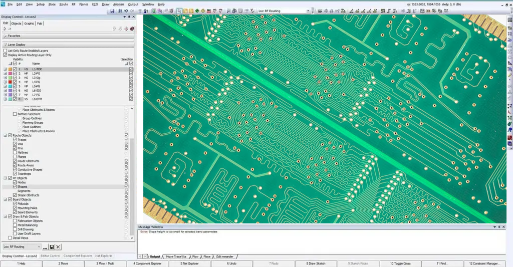
High-Speed PCB
In today’s electronic devices, high-speed integrated circuits need precisely designed PCBs to operate efficiently. Mars PCB provides specialized PCB manufacturing services that ensure tight tolerances and the best materials for high-speed designs. By focusing on signal integrity, Mars PCB helps you create PCBs that meet the demands of cutting-edge technology.
As technology advances, signal frequencies and data rates increase, making it challenging for engineers to maintain signal integrity and performance. High-speed PCB design is essential for modern devices.
Mars PCB is dedicated to providing the best guidelines for high-speed PCBs. Below, you’ll find what these PCBs are, some design tips to get you started, and more.
What is High-Speed PCB Design?
High-speed PCB design involves creating printed circuit boards that effectively handle high-frequency signals and rapid digital transitions.
Unlike traditional PCB design, high-speed PCB design emphasizes maintaining signal integrity and controlling impedance. It also minimizes electromagnetic interference (EMI) in circuits operating at frequencies typically above 50 to 100 MHz or with rise times below 1 nanosecond.
Key Components of High-Speed PCB Design
Consider the following key aspects for high-speed PCBs:
- Careful PCB stackup design
- Proper use of ground and power planes
- Controlled impedance traces
- Management of signal reflections and crosstalk
- Attention to return paths and transmission line effects
Applications of High-Speed Circuit Boards
High-speed PCBs are vital for various applications:
- High-performance computing
- Telecommunications equipment
- Advanced networking devices
- High-definition video systems
- Radar and RF applications
High-Speed PCB Design Guidelines
Follow these PCB design tips to ensure optimal performance for your device
Trace Length and Routing
Keep high-speed traces as short as possible to reduce signal degradation. Use length matching for differential pairs and parallel bus signals. Avoid right-angle bends in traces; instead, use 45° bends or curved corners.
Spacing and the 3W Rule
Ensure adequate spacing between traces to minimize crosstalk. Follow the 3W rule by keeping the space between adjacent traces at least three times the trace width. Increase spacing for critical or sensitive signals.
Board Stackup
Design an appropriate PCB stackup with alternating signal and plane layers. Use symmetrical stackups to prevent board warping during manufacturing. Consider high-frequency PCB dielectric materials for critical layers.
Example of a 6-layer high-speed PCB stackup
Layer | Type |
1 | Signal |
2 | Ground Plane |
3 | Signal |
4 | Power Plane |
5 | Signal |
6 | Ground Plane |
High-Speed PCB Design Considerations
- Signal Integrity: Monitor signal quality throughout the PCB using simulation tools before fabrication.
- EMI/EMC: Implement proper shielding and grounding techniques to ensure electromagnetic compatibility.
- Power Distribution Network (PDN): Design a reliable PDN to provide clean power to all components. Use decoupling capacitors to reduce power supply noise.
- Manufacturing and Testing: Design for manufacturability and testability, including impedance testing and signal integrity verification.
- Transmission Line Effects: Address transmission line behavior, including reflections, ringing, and signal distortion.
- Thermal Management: Consider heat dissipation and use proper thermal management techniques.
- Layer Stackup: Optimize the PCB stackup for signal integrity and impedance control. Choose appropriate dielectric materials for high-speed applications.
- Component Placement: Carefully place components to minimize PCB trace lengths and group related components to enhance digital signal integrity.
Keeping these considerations in mind ensures your board is reliable and performs optimally. Refer to this list during your design process for the best results!

What is High-Speed PCB Design?
Wondering if your PCB requires a high-speed layout to enhance performance? Here are some indicators
High-Speed PCB Design Considerations
If your design includes high-speed interfaces like PCI-e, DDR, or video interfaces such as DVI and HDMI, a high-speed circuit board layout is necessary. These interfaces require adherence to high-speed design rules.
Trace Length and High-Speed Signal Wavelength
When the wavelength of your signals is comparable to the trace length, a high-speed design is essential. Standards like DDR require traces to be length-matched within tight tolerances.
Wireless Interfaces
If your board features an antenna directly on the board or through a connector, a high-speed design is needed for digital signals. Onboard antennas require precise impedance matching and length tuning. Boards with SMA connectors or similar require traces with specific impedance values, necessitating a high-speed PCB design and layout.
Mars PCB: Specialized PCB Manufacturing Services
High-speed PCB designs handle high-frequency signals and rapid digital transitions efficiently. They are ideal for demanding environments where maintaining signal integrity and controlling impedance are crucial.
With the right manufacturing partner, you can trust that your designs will be transformed into precise physical products.
Mars PCB is a leading PCB manufacturing and assembly company offering global service and support. We tackle the challenges of high-speed design to ensure you receive a high-quality product. For more information, reach out to our friendly team!
What is High-Speed PCB Design? Helpful Guidelines FAQs
A high-speed circuit typically operates with clock frequencies above 50 to 100 MHz or with signal rise times below 1 nanosecond. These circuits require special design rules to maintain signal integrity and prevent electromagnetic interference.
High-speed signals have faster rise times and higher frequencies compared to low-speed signals, resulting in more complex behavior on the PCB. Low-speed signals are simple point-to-point connections, while high-speed signals are transmission lines with impedance control and meticulous PCB routing.
The top three crucial steps in PCB design and layout are:
Proper Component Placement:Optimizes signal flow and minimizes trace lengths.
Careful Stackup Design:Ensures controlled impedance and signal integrity.
Efficient Trace Routing:Addresses signal integrity and EMI issues through optimal routing paths.
Ready to elevate your electronic designs with cavity PCB technology?
Contact MarsPcb today for a consultation with our expert engineers and discover how our advanced manufacturing capabilities can bring your next-generation products to life.