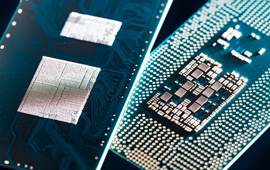
In the fast-paced world of modern electronics, where data flows at unprecedented rates, the integrity of signals is paramount. From sophisticated data centers to cutting-edge 5G infrastructure and advanced AI systems, the demand for high-speed PCB technology is exploding. But designing PCBs that can reliably handle these extreme speeds isn’t just about pushing electrons faster; it’s a complex interplay of physics, materials science, and meticulous engineering. One of the most critical, yet often underestimated, aspects of this complexity is Electromagnetic Interference (EMI) and the vital role of effective shielding. This article delves into the intricacies of high-speed PCB design and explores how well-implemented EMI shielding can make or break your next-generation electronic products.
I. Introduction to High-Speed PCB Design
A. What Defines a High-Speed PCB?
A high-speed PCB isn’t simply defined by its operating frequency, but more critically by the rise time of its signals. If the signal’s rise time is comparable to or shorter than the propagation delay across the trace, then transmission line effects become significant, and the board is considered “high-speed.” This means traditional “low-speed” design rules simply won’t cut it. Signal integrity becomes the cornerstone of every design decision, focusing on minimizing distortion, reflections, and attenuation.
B. Why High-Speed Design Matters
The consequences of poor high-speed PCB design can be severe, leading to everything from intermittent data errors and system instability to catastrophic compliance failures. Imagine a 5G base station unable to maintain stable connections, or an AI accelerator producing erroneous computations—these are direct results of neglecting high-speed principles. The ultimate goal is to ensure that signals arrive at their destination accurately and within timing specifications, thus guaranteeing the robust performance and reliability of the electronic system.
C. Common Challenges in High-Speed PCB Design
The journey to a successful high-speed PCB is fraught with challenges:
- Signal Attenuation and Distortion: Signals lose strength and change shape as they travel, especially over long traces.
- Crosstalk: Unwanted coupling of signals between adjacent traces, leading to interference.
- Power Integrity Issues: Fluctuations in power and ground planes (e.g., ground bounce, power rail noise) can directly impact signal quality.
- Electromagnetic Interference (EMI): The unwanted emission or reception of electromagnetic energy, a major cause of system malfunction and compliance issues.
II. Fundamentals of High-Speed Signal Integrity
Achieving pristine signal integrity requires a deep understanding of several fundamental concepts.
A. Transmission Line Theory in Practice
At high speeds, PCB traces behave like transmission lines, not just simple wires. This means characteristic impedance matching is crucial. Any mismatch creates reflections that bounce back and forth, distorting the signal. Termination schemes (e.g., series, parallel, AC termination) are employed to absorb these reflections and ensure signals travel cleanly.
B. Controlled Impedance Routing
Maintaining consistent controlled impedance routing across the board is fundamental.
- Microstrip vs. Stripline: Microstrip traces are on outer layers, while striplines are embedded between ground planes. Each has different impedance characteristics and propagation delays.
- Trace Geometry and Dielectric Constant: Trace width, thickness, and the dielectric constant of the PCB material directly influence impedance. Precision in manufacturing is key here, which is why choosing a reputable high-speed PCB supplier is critical.
C. Via Design Considerations
Vias, while necessary for layer transitions, can degrade signal integrity.
- Stubs and Anti-pads: Unused portions of vias (stubs) can cause reflections. Back-drilling is a technique used to remove these stubs, crucial for signals above a few GHz.
- Anti-pads: Oversized clearances around vias in ground planes can create slots, impacting return current paths.
D. Crosstalk Management
Minimizing crosstalk is essential. This involves adhering to strict spacing rules between traces and careful differential pair routing. For highly sensitive signals, shielded traces (traces flanked by ground guards) can offer an additional layer of protection.
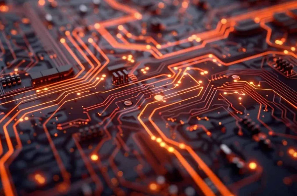
III. Understanding Electromagnetic Interference (EMI) in High-Speed PCBs
EMI is the silent killer of performance in high-speed systems. It’s an issue that must be addressed proactively, not reactively.
A. Sources of EMI in High-Speed Designs
- Switching Noise: The rapid switching of digital circuits generates broadband noise.
- Radiation from Traces and Components: Long traces can act as antennas, radiating electromagnetic energy.
- Ground Loops and Common-Mode Currents: Unintended current paths can create radiating loops.
B. How EMI Affects System Performance
EMI can manifest as data corruption, increased bit errors, reduced signal-to-noise ratio (SNR), and, critically, compliance failures with regulatory bodies like FCC and CE. These failures can lead to significant delays and costs.
C. Near-Field vs. Far-Field EMI
Understanding the distinction helps in mitigation. Near-field EMI (magnetic and electric field coupling) is close to the source, often managed by good layout and grounding. Far-field EMI, which radiates as electromagnetic waves, requires shielding to prevent external interference and internal emissions.
IV. The Critical Role of EMI Shielding in High-Speed PCBs
Effective EMI shielding is not just an add-on; it’s an integral part of high-speed PCB manufacturing and design.
A. Principles of EMI Shielding
Shielding works primarily through reflection (bouncing electromagnetic waves off a conductive surface) and absorption (dissipating energy as heat within the shield material). The concept of a Faraday cage—an enclosure that blocks external static and non-static electric fields—is fundamental to understanding effective shielding.
B. Types of EMI Shielding Solutions for PCBs
| Shielding Type | Description | Common Materials / Examples |
| On-Board Shielding | Discrete metal cans or enclosures mounted directly onto the PCB. | Copper, nickel-silver, stainless steel. |
| Board-Level Shielding | Integrated into the PCB design or assembly. | Shielded connectors, buried ground planes, conductive coatings. |
| Component-Level Shielding | Shields applied directly to individual sensitive components. | Shielded inductors, ferrite beads, common-mode chokes. |
- 1. On-Board Shielding (e.g., Shielding Cans/Enclosures): These are often the most visible form of shielding.
- Material Considerations: Copper offers excellent conductivity, while nickel-silver provides good strength and corrosion resistance.
- Grounding Techniques: Proper grounding of the shield to the PCB’s ground plane is paramount. An ungrounded shield is essentially an antenna.
- Ventilation and Thermal Management: Enclosed shields can trap heat, necessitating careful design for airflow.
- 2. Board-Level Shielding (e.g., Integrated Shielding):
- Shielded Connectors and Cables: Preventing EMI from entering or exiting via I/O.
- Embedded Shielding Layers: Dedicated ground planes within the PCB stackup act as internal shields, common in advanced china high-speed pcb manufacturing.
- Conformal Coating and Conductive Paints: Offer broad area shielding, especially for odd-shaped components.
- 3. Component-Level Shielding:
- Shielded Inductors and Transformers: Components that inherently radiate or are sensitive to EMI can be purchased with integrated shielding.
- Ferrite Beads and Common-Mode Chokes: Used to suppress high-frequency noise on power and signal lines.
C. Design Considerations for Effective EMI Shielding
Effective EMI shielding goes beyond simply placing a metal box; it requires careful design to prevent gaps and ensure a continuous conductive path.
- Seam Integrity and Aperture Control: Gaps, holes, or poorly sealed seams can act as slots, allowing EMI to escape or enter.
- Grounding Strategy: The shield must be thoroughly grounded to the system’s reference potential.
- Impact on Thermal Dissipation: Shielding can trap heat, so thermal simulations are often necessary.
- Manufacturing Feasibility and Cost: Balancing optimal shielding with practical manufacturing techniques and budget constraints is crucial. This is where expertise from a seasoned high-speed PCB supplier really pays off.
V. Integrating EMI Shielding into High-Speed PCB Design Workflow
EMI shielding isn’t an afterthought; it’s a fundamental aspect of the high-speed PCB design process.
A. Early Design Stage Considerations
- Stack-up Planning: A well-designed stack-up with strategically placed ground planes forms the foundation for effective EMI control.
- Component Placement: Sensitive components should be placed away from noisy ones, and critical signal paths should be isolated.
- Power Distribution Network (PDN) Design: A robust PDN minimizes ground bounce and power rail noise, reducing a significant source of EMI.
B. Simulation and Analysis for EMI
Before manufacturing, EMI/EMC simulation tools (e.g., 3D field solvers) are invaluable for predicting potential EMI issues. Pre-compliance testing can save significant time and money by identifying problems early, avoiding costly redesigns and re-spins.
C. Best Practices for High-Speed Routing with Shielding
- Strategic Placement of Ground Vias for Shields: Ensure solid, low-impedance connections for all shield elements to the ground plane.
- Managing Openings in Ground Planes: Avoid large, unbroken slots in ground planes that can disrupt return current paths and act as radiating antennas.
- Differential Pair Routing with Guard Traces: For critical differential signals, surrounding them with grounded guard traces provides isolation from external interference and confines their own fields.
VI. Common User Questions and Troubleshooting
Here are some frequently asked questions from engineers embarking on high-speed PCB projects:
A. “Do I always need EMI shielding for high-speed designs?”
Not always, but often. The necessity depends on factors like clock frequency, data rates, the application’s sensitivity, and regulatory requirements (e.g., FCC Class B). For most designs exceeding 100 MHz or involving sensitive analog components, some form of EMI mitigation, including shielding, is highly recommended.
B. “How do I choose the right shielding material?”
The choice depends on the type of field (electric or magnetic), frequency, cost, and environmental factors. Generally, materials with high conductivity (like copper or aluminum) are good for electric fields, while materials with high permeability (like steel or Mu-metal) are better for magnetic fields. Often, composite materials are used for a broader range of protection.
C. “Will shielding affect my signal integrity?”
Improperly implemented shielding certainly can. If a shield is poorly grounded or creates unintended capacitive or inductive coupling paths, it can degrade signal integrity. However, when designed correctly, shielding enhances signal integrity by reducing external noise and crosstalk, allowing signals to maintain their fidelity.
D. “What are the common pitfalls in implementing EMI shielding?”
The most frequent mistakes include:
- Poor grounding of shields: This creates antennas instead of shields.
- Unsealed seams or large apertures: EMI leaks through these openings.
- Inadequate ventilation: Leading to thermal issues.
- Ignoring return path integrity: Disrupting return currents can nullify shielding efforts.
E. “How can I test the effectiveness of my EMI shielding?”
- Anechoic chamber testing: The gold standard for radiated emissions and immunity testing.
- Near-field probe measurements: Useful for pinpointing sources of EMI on the PCB itself.
- Spectrum analyzer measurements: To identify noise peaks and their frequencies.
VII. Conclusion
High-speed PCB design is a challenging but rewarding endeavor, and the impact of EMI shielding cannot be overstated. From selecting the right high-speed PCB supplier and ensuring robust high-speed PCB manufacturing processes to meticulously implementing shielding strategies, every step is crucial. By understanding the fundamentals of signal integrity, recognizing the pervasive nature of EMI, and adopting proactive shielding techniques, engineers can confidently design and deliver reliable, high-performance electronic systems. As technology continues to accelerate, the synergy between meticulous high-speed PCB design and intelligent EMI mitigation will remain at the forefront of innovation.