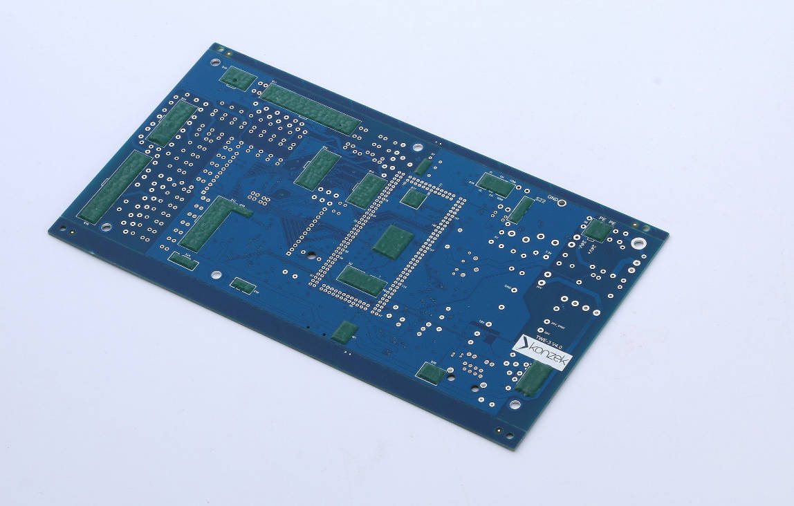
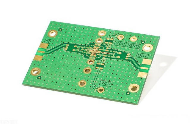
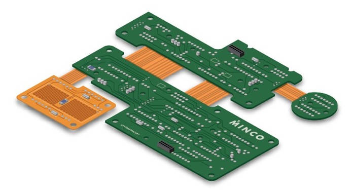
In high-speed PCB design, the choice between increasing copper thickness versus trace width is a critical balancing act dictated by the specific application’s needs. Generally, wider traces are preferred for controlling impedance and ensuring signal integrity in high-speed data lines, while thicker copper is primarily used to increase the current-carrying capacity and improve thermal management for power lines. Mastering this trade-off is fundamental to designing a reliable, high-performance circuit board that avoids issues like signal degradation, overheating, and manufacturing defects.
Table of Contents
- Understanding the Fundamentals: What Are We Comparing?
- The Core Conflict: Power Integrity vs. Signal Integrity
- How Do High-Speed Effects Influence the Choice?
- Practical Considerations: Design for Manufacturability (DFM) and Cost
- The Verdict: A Decision-Making Framework
- Tools and Calculators for Accurate Design
- Conclusion: A Symbiotic Relationship, Not a Rivalry
- Frequently Asked Questions (FAQ)
Understanding the Fundamentals: What Are We Comparing?
Before diving into the complex trade-offs, it’s essential to establish a clear understanding of the two primary variables at play. While they both define the cross-sectional area of a conductor, they have vastly different implications for electrical performance and manufacturability.
What is Copper Thickness (Copper Weight)?
Copper thickness, often referred to as copper weight, specifies the thickness of the copper foil on a PCB’s inner and outer layers. It is most commonly measured in ounces per square foot (oz/ft²). For instance, “1 oz copper” means that one ounce of copper is spread evenly over a one-square-foot area, resulting in a thickness of approximately 1.37 mils or 35 micrometers (μm).
- Standard Thickness: 1 oz (35μm) and 0.5 oz (18μm) are the most common for standard signal layers.
- Heavy Copper: Anything 2 oz (70μm) or greater is considered heavy copper, used primarily for high-current applications.
- Impact: Thicker copper directly increases the cross-sectional area of a trace, significantly boosting its ability to carry current and dissipate heat. However, it also presents challenges in etching fine lines and spaces.
What is Trace Width?
Trace width is the horizontal dimension of a copper trace on the PCB layer, typically measured in mils (thousandths of an inch) or millimeters (mm). This dimension is a primary tool for designers to control electrical characteristics. It can be easily adjusted within EDA (Electronic Design Automation) software for each specific net.
- Flexibility: Unlike copper thickness, which is typically uniform across an entire layer, trace width can be varied from trace to trace.
- Impact: Wider traces reduce resistance and increase current capacity, similar to thicker copper. Crucially for high-speed design, trace width, in conjunction with the dielectric height and material, is the primary lever for controlling characteristic impedance.

The Core Conflict: Power Integrity vs. Signal Integrity
The decision to prioritize copper thickness or trace width almost always comes down to answering one question: Is this trace’s primary job to deliver clean power or to transmit high-fidelity data? The answer determines your optimization strategy.
Scenario 1: Optimizing for Power Integrity and Current Capacity
When designing power planes, power delivery networks (PDNs), or traces for motors and high-power components, the primary concern is ampacity—the maximum current a conductor can carry before its temperature rises to an unacceptable level. Here, both thickness and width contribute to increasing the cross-sectional area, which lowers DC resistance and improves heat dissipation.
The industry standard for calculating this is governed by IPC standards, primarily IPC-2152: Standard for Determining Current-Carrying Capacity in Printed Board Design. This newer standard provides a more comprehensive model than the older IPC-2221 by considering the thermal effects of the board material and nearby planes.
When to use thicker copper:
- Space is limited: When you cannot make a trace wider due to routing density, increasing the copper weight from 1 oz to 2 oz can effectively double the current capacity for a similar temperature rise without consuming more board space.
- Thermal Management: Heavy copper acts as an excellent heat sink, pulling heat away from components and distributing it across the board, which is vital for power electronics.
When to use wider traces:
- Cost-sensitive designs: Increasing trace width is “free” in terms of material cost, whereas specifying thicker copper adds a premium to the PCB fabrication cost.
- Standard processes: Using a standard 1 oz copper process and simply widening power traces keeps the design within the most common and cost-effective manufacturing capabilities.
Scenario 2: Optimizing for Signal Integrity and Impedance Control
For high-speed signals (e.g., USB, Ethernet, DDR memory, RF signals), the trace is not just a simple conductor; it’s a transmission line. The most critical parameter is its characteristic impedance (Z₀), which must match the impedance of the driver and receiver to prevent signal reflections that cause data corruption.
Impedance is determined by the physical geometry of the trace:
- Trace width (W)
- Copper thickness (T)
- Dielectric height (H) – the distance to the reference plane
- Dielectric constant (Er) of the PCB material
In this context, trace width (W) is the most influential and easily controlled parameter for tuning impedance. While copper thickness (T) does factor into the calculation, its effect is less pronounced than that of width and dielectric height. For high-speed signals, designers often prefer *wider, thinner traces* on a standard 0.5 oz or 1 oz copper layer. This geometry provides better control over the target impedance and minimizes signal loss.
How Do High-Speed Effects Influence the Choice?
As signal frequencies climb into the MHz and GHz ranges, physical phenomena emerge that further favor width adjustments over thickness for signal lines.
The Skin Effect: Why Width Often Wins for High Frequencies
At high frequencies, AC current does not flow through the entire cross-section of a conductor uniformly. Instead, it tends to concentrate on the outer surface, or “skin,” of the trace. This phenomenon is known as the skin effect. Because the inner core of the copper is underutilized, simply making the copper thicker provides diminishing returns for reducing AC resistance.
However, by making the trace wider, you increase the surface area where the current can flow, which more effectively reduces signal loss (attenuation) at high frequencies. This makes trace width a much more potent tool than copper thickness for combating skin effect losses in multi-gigabit signal paths.
Characteristic Impedance Control: A Game of Geometry
Maintaining a constant impedance (e.g., 50 ohms for single-ended signals or 100 ohms for differential pairs) is paramount. Field solver tools within EDA software calculate this based on the stackup geometry. When designing, you typically start with a fixed copper thickness (e.g., 1 oz) and dielectric height, then solve for the required trace width. For example, to achieve a 50 Ω impedance on a standard FR-4 board, a trace might need to be 7 mils wide. Changing the copper thickness to 2 oz would slightly alter this calculation, but the primary tuning knob remains the trace width.
Impact on Differential Pairs
For differential pairs, both the trace width and the spacing between the two traces must be tightly controlled to maintain the target differential impedance (e.g., 90 Ω or 100 Ω). Using excessively thick copper can make it difficult for fabricators to maintain consistent spacing and trace profiles, potentially degrading the signal quality. A thinner, more precisely etched trace provides better performance for tightly coupled differential pairs.
Practical Considerations: Design for Manufacturability (DFM) and Cost
The optimal design on paper is useless if it cannot be reliably and affordably manufactured. This is where practical constraints often guide the decision.
Etching Tolerances and the Trapezoidal Effect
PCB traces are created by chemically etching away unwanted copper. This process is not perfectly vertical. As the etchant works its way down, it also etches sideways, resulting in a trace that has a trapezoidal, rather than a perfectly rectangular, cross-section. This effect is far more pronounced with thicker copper.
For a 2 oz copper layer, the undercut can be significant, making it very difficult to create fine traces and small spaces. A common rule of thumb is that the minimum trace width and space should be greater than the copper thickness. Trying to route an 4-mil trace on a 2 oz (2.8 mils thick) copper layer is not feasible for most fabricators. Therefore, for dense, high-speed designs requiring fine lines (like BGA breakouts), thinner copper (0.5 oz or 1 oz) is mandatory.
Cost Implications of Thicker Copper
PCB fabrication costs are directly influenced by material usage and process complexity.
- Material Cost: Copper is a commodity, so thicker copper foils cost more.
- Process Cost: Heavy copper requires longer etching times, more specialized processes, and often results in lower yields, all of which increase the final price of the board.
In contrast, adjusting trace width within standard manufacturing limits has no impact on the board’s cost, making it the more economical choice whenever possible.
The Verdict: A Decision-Making Framework
There is no universal winner. The choice is application-dependent. Use this table as a guide to determine which parameter to prioritize.
| Design Goal | Primary Concern | Prioritize… | Reasoning |
|---|---|---|---|
| High-Speed Signal (e.g., USB 3.0, PCIe) | Signal Integrity, Impedance Control | Trace Width | Width is the primary factor for impedance. It also helps combat skin effect. Thinner copper (0.5oz/1oz) allows for finer, more precise etching. |
| Power Delivery (e.g., VRM, Motor Drive) | Current Capacity (Ampacity), Thermal Management | Copper Thickness | Thicker copper dramatically increases current capacity for a given width, providing a space-efficient solution and excellent heat dissipation. |
| High-Density Routing (e.g., BGA breakout) | Space Constraints, Manufacturability | Thinner Copper (and narrow traces) | Thinner copper (e.g., 0.5 oz) is essential to achieve the fine trace widths and spacings required for dense component packages. |
| Cost-Sensitive Project | Minimizing Fabrication Cost | Wider Traces on Standard Copper | Using a standard 1 oz copper process and widening traces where needed is more economical than specifying a more expensive heavy copper process. |
Tools and Calculators for Accurate Design
Never rely on guesswork. Professional PCB design relies on powerful tools to model performance accurately:
- PCB Trace Width Calculators: Many online tools and integrated EDA features use IPC-2152 formulas to calculate the required trace width for a target current and temperature rise.
- Field Solvers: Integrated into high-end EDA software (like Altium Designer, Cadence Allegro), these tools accurately calculate characteristic impedance by modeling the electromagnetic fields around the trace, accounting for width, thickness, stackup, and nearby conductors.
- Fabricator DFM Rules: Always consult your chosen manufacturer’s design rules. They will specify their capabilities regarding minimum trace/space for different copper weights.
Conclusion: A Symbiotic Relationship, Not a Rivalry
Ultimately, copper thickness and trace width are not adversaries but rather two complementary parameters in the PCB designer’s toolkit. The art of high-speed design lies in understanding their distinct roles. For signals, think in terms of geometry for impedance—where trace width is king. For power, think in terms of cross-sectional area for current—where both width and thickness are powerful allies. By making informed, application-specific decisions, you can achieve a design that is not only electrically superior but also robust, reliable, and manufacturable.
Frequently Asked Questions (FAQ)
1. Is 2 oz copper better than 1 oz copper for high-speed signals?
No, not necessarily. While 2 oz copper has lower DC resistance, for high-speed signals, the downsides often outweigh the benefits. The pronounced skin effect means the extra thickness is underutilized at high frequencies, and the difficulty in etching precise trace geometries can lead to worse impedance control and signal integrity. For most high-speed applications, 1 oz or 0.5 oz copper is preferred.
2. How much current can a 10 mil trace handle?
This depends heavily on the copper thickness and the acceptable temperature rise. According to IPC-2152 calculators, a 10 mil trace on an external layer of 1 oz copper might handle around 1A for a 10°C temperature rise. On a 2 oz copper layer, the same trace could handle closer to 1.5A under similar conditions.
3. Does copper thickness affect signal speed?
Not directly. The propagation speed of a signal is primarily determined by the dielectric constant (Er) of the PCB material. However, copper thickness can affect signal integrity and attenuation (signal loss), which can impact the maximum usable frequency or distance of a link. Poor impedance control caused by imprecise etching on thick copper can degrade the signal and cause data errors, effectively limiting the performance.
High-Speed PCB Design, Copper Thickness vs Trace Width, PCB Trace Impedance, PCB Current Carrying Capacity, PCB Signal Integrity, 1 oz vs 2 oz copper pcb, PCB trace width calculation, skin effect in pcb traces, controlled impedance pcb, pcb design for manufacturability, heavy copper pcb, what is copper weight in pcb


