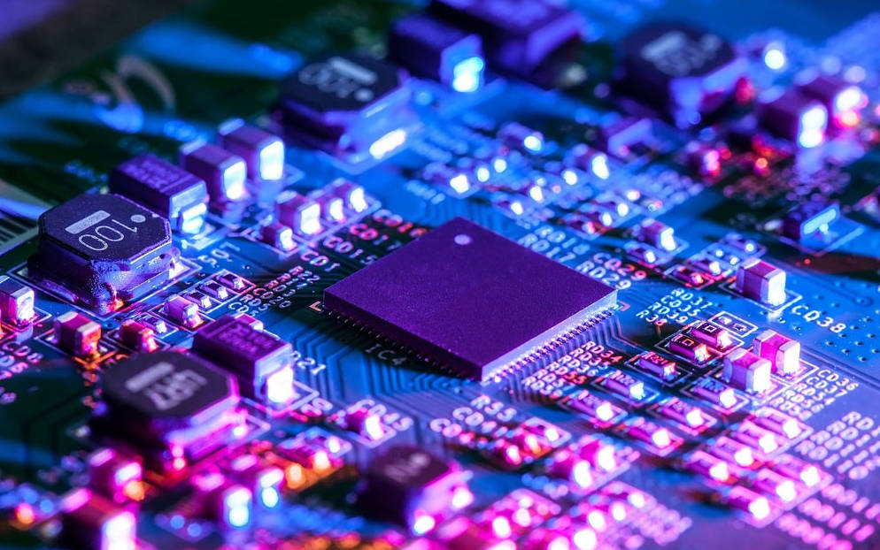
The key difference between a high-speed PCB and an RF PCB lies in their primary design goal and the nature of the signals they handle. High-speed PCBs are designed to maintain the signal integrity of fast-switching digital signals, focusing on timing, preventing distortion, and managing high-frequency harmonics. In contrast, RF (Radio Frequency) PCBs are engineered to manage and transmit high-frequency analog signals efficiently, focusing on precise impedance matching for maximum power transfer and minimizing signal loss through wave propagation. While both deal with high frequencies, their design principles, materials, and challenges are fundamentally distinct, catering to the digital world of data versus the analog world of radio waves.
Table of Contents
- What is a High-Speed PCB? The World of Digital Signal Integrity
- What is an RF PCB? Mastering Analog Wave Propagation
- Head-to-Head Comparison: High-Speed PCB vs. RF PCB
- Key Differentiator: Materials and Substrates
- The Convergence Zone: When High-Speed and RF Designs Overlap
- Which PCB is Right for Your Project? A Decision-Making Guide
- Conclusion: Choosing the Right Path for Performance
What is a High-Speed PCB? The World of Digital Signal Integrity
A printed circuit board is generally classified as “high-speed” not merely because of its clock frequency, but because the integrity of the digital signals it carries is affected by the physical characteristics of the board itself. The primary concern in high-speed design is signal integrity. As the rise and fall times of digital pulses (square waves) become shorter, they begin to behave less like simple DC signals and more like high-frequency transmission lines. This means that factors like trace length, width, proximity to other traces, and board material can introduce a host of problems.
The main goal is to ensure that a digital signal—a ‘1’ or a ‘0’—arrives at its destination at the correct time and with a clean, recognizable shape. Any degradation, such as ringing, crosstalk, or reflections, can lead to data errors, system instability, and functional failure. Therefore, high-speed PCB design is a meticulous practice of managing impedance, controlling signal timing (skew), and mitigating electromagnetic interference (EMI).
Defining Characteristics of High-Speed Design
- Focus on Rise/Fall Time: The speed of a digital signal is more about how quickly it transitions between states (its edge rate) than the clock frequency itself. A slow clock signal with a very fast rise time can exhibit high-speed effects.
- Controlled Impedance: Traces are designed as transmission lines with a specific characteristic impedance (typically 50 ohms single-ended) to prevent signal reflections that corrupt the data.
- Signal Integrity (SI) Analysis: Designers use advanced simulation tools to analyze and prevent issues like crosstalk (unwanted coupling between traces), skew (timing mismatches in differential pairs), and attenuation.
- Differential Signaling: Techniques like using differential pairs (e.g., for USB, HDMI, Ethernet) are common to improve noise immunity and reduce EMI.
Common Applications for High-Speed PCBs
High-speed PCBs are the backbone of the modern digital world. You can find them in virtually any device that processes large amounts of data quickly, including:
- Computer motherboards and graphics cards
- Servers, routers, and network switches
- Solid-State Drives (SSDs)
- High-resolution video processing equipment
- Telecommunications infrastructure
What is an RF PCB? Mastering Analog Wave Propagation
An RF (Radio Frequency) PCB is designed to operate on analog signals in the megahertz (MHz) to gigahertz (GHz) frequency range. Unlike the on/off nature of digital signals, RF signals are continuous analog waves. The primary objective of an RF PCB design is not just to get a signal from point A to B, but to do so with maximum power transfer and minimal loss or distortion. In the RF world, the PCB is not just a substrate for mounting components; it is an active part of the circuit itself. Traces, vias, and even the ground planes behave as circuit elements like inductors and capacitors.
Designers of RF PCBs are fundamentally concerned with managing electromagnetic fields and wave propagation. They must account for phenomena that are less critical in lower-frequency or purely digital designs, such as the skin effect (where current flows on the surface of a conductor) and dielectric loss (where the board material itself absorbs signal energy). Every millimeter of the layout can impact performance, making RF design a highly specialized discipline.
Defining Characteristics of RF Design
- Precise Impedance Matching: While also important in high-speed design, impedance matching in RF is critical for maximizing power transfer between components (like an amplifier and an antenna) and minimizing Voltage Standing Wave Ratio (VSWR).
- Low-Loss Materials: Standard FR-4 material has high dielectric loss at RF frequencies. RF PCBs require specialized substrates like Rogers, Teflon (PTFE), or ceramic with stable dielectric constants (Dk) and low dissipation factors (Df).
- Mitigation of Parasitics: Designers must meticulously control parasitic capacitance and inductance from pads, traces, and vias, as these can drastically alter circuit performance at high frequencies.
- EM Field Management: Layout techniques focus on containing electromagnetic fields, preventing radiation, and ensuring proper grounding and shielding to isolate sensitive circuit sections.
Common Applications for RF PCBs
RF circuits are essential for any wireless technology. Key applications include:
- Smartphones, tablets, and Wi-Fi routers (antennas and front-end modules)
- Bluetooth devices and IoT sensors
- Radar systems (automotive, aerospace)
- GPS receivers and satellite communication systems
- Wireless power transfer systems
Head-to-Head Comparison: High-Speed PCB vs. RF PCB
To truly understand the differences, it’s helpful to compare these two PCB types across several key design parameters. While there is some overlap, their priorities and solutions diverge significantly.
| Feature | High-Speed PCB | RF PCB |
|---|---|---|
| Primary Goal | Signal Integrity: Preserve the timing and shape of digital pulses. | Power Transfer & Purity: Transmit analog signals with minimal loss and distortion. |
| Signal Type | Digital (square waves with fast rise/fall times). | Analog (continuous sine waves). |
| Frequency Concern | Concerned with the high-frequency harmonics contained within the fast edge rate of a digital signal. | Concerned with the fundamental carrier frequency of the analog signal. |
| Impedance Control | To prevent reflections and maintain signal waveform. Tolerance is typically around ±10%. | To achieve maximum power transfer. Tolerance is often much tighter, around ±1% to ±5%. |
| Key Metrics | Eye diagrams, jitter, skew, crosstalk. | S-parameters (S11, S21), VSWR, noise figure, phase noise. |
| Layout Focus | Trace length matching, routing density, via design, power plane integrity. | Trace geometry (microstrip, coplanar waveguide), minimizing sharp corners, shielding, ground stitching. |
Key Differentiator: Materials and Substrates
Perhaps the most tangible difference between high-speed and RF boards is the material they are built on. The choice of substrate is dictated by two critical properties: the dielectric constant (Dk) and the dissipation factor (Df), also known as loss tangent.
- Dielectric Constant (Dk): This value affects the impedance and propagation speed of signals on the PCB. For RF circuits, it is crucial that the Dk is extremely stable across a wide range of frequencies to ensure predictable performance. Any variation can detune filters or mismatch impedances.
- Dissipation Factor (Df): This measures how much signal energy is absorbed and lost as heat within the substrate material. Standard FR-4 has a relatively high Df, which is unacceptable for many RF applications where every fraction of a decibel (dB) of signal loss matters.
Consequently, while some high-speed digital designs can use high-performance FR-4, RF designs almost exclusively rely on specialized laminates. Materials from manufacturers like Rogers, Taconic, or Arlon offer significantly lower Df and more stable Dk, but they come at a much higher cost and require specialized manufacturing processes. This material choice is a fundamental trade-off between performance and cost that engineers must navigate.
The Convergence Zone: When High-Speed and RF Designs Overlap
The line between high-speed digital and RF is becoming increasingly blurred in modern electronics. A perfect example is a Wi-Fi or 5G module. Such a device contains a high-speed digital processor that handles data, which then feeds a complex RF front-end that transmits and receives wireless signals. These are often built on a single “mixed-signal” PCB.
Designing these hybrid boards presents a unique challenge. The noisy, fast-switching digital section must be carefully isolated from the highly sensitive analog RF section. This involves meticulous grounding strategies, physical separation, shielding cans, and careful power supply filtering to prevent digital noise from corrupting the RF signals. The board may even use different materials in different sections—a technique known as hybrid PCB construction—to optimize performance for both domains while managing cost.
Which PCB is Right for Your Project? A Decision-Making Guide
Choosing the correct design approach depends entirely on your application’s primary function. Ask yourself these key questions:
- What is the nature of my signal? If you are dealing with data buses, memory interfaces, or fast-switching logic (square waves), you are in the realm of high-speed digital design. If you are working with antennas, filters, amplifiers, or mixers (sine waves), you need an RF design approach.
- What is my main performance concern? Is it ensuring data bits arrive uncorrupted and on time? That’s a signal integrity problem, pointing to high-speed design. Is it minimizing signal loss over distance or maximizing the power delivered to an antenna? That’s an RF problem.
- What frequency defines my problem? For digital signals, the “knee frequency” (related to the signal’s rise time) determines if high-speed rules apply. For analog, it’s the fundamental operating frequency (e.g., 2.4 GHz for Wi-Fi) that dictates the design rules and material selection.
Conclusion: Choosing the Right Path for Performance and Reliability
In summary, while both high-speed and RF PCBs operate at high frequencies, they serve different masters. High-speed PCB design is a discipline dedicated to preserving the integrity of digital data, battling against timing errors and signal distortion. RF PCB design is an art of managing analog electromagnetic waves, focusing on power efficiency and signal purity. Understanding this core distinction—digital signal integrity versus analog power transfer—is the first and most critical step in selecting the right materials, design rules, and manufacturing techniques to ensure your electronic product performs reliably and effectively in its intended application.
High-Speed PCB vs RF PCB, difference between high-speed and rf pcb, high-speed pcb design, rf pcb materials, what is a high-speed pcb, radio frequency pcb, signal integrity vs power transfer, pcb design guidelines, high-frequency pcb

