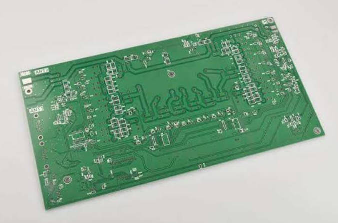
Choosing a high frequency PCB manufacturer is not the same as selecting a supplier for standard FR-4 circuit boards. RF and microwave applications are more sensitive to dielectric loss, impedance variation, copper roughness, layer registration, drilling accuracy, plating quality, and fabrication consistency.
A qualified high frequency PCB manufacturer should understand RF materials, impedance control, lamination behavior, copper surface quality, and testing requirements before moving a design into production. For engineers and buyers, the key is not only whether a factory can “make the board,” but whether it can manufacture the PCB without damaging signal integrity, increasing insertion loss, or introducing uncontrolled performance variation.
This guide explains how to evaluate a manufacturer for RF PCB and microwave PCB projects, what technical factors matter, what questions to ask before ordering, and how to prepare your Gerber files for quotation.
For projects involving RF circuits, antenna modules, microwave communication systems, radar electronics, or high-speed signal transmission, you can also review high frequency PCB manufacturing options from Mars-PCB.
What Is a High-Frequency PCB?
A high-frequency PCB is a printed circuit board designed to carry high-speed, RF, microwave, or millimeter-wave signals with controlled electrical performance. Unlike general-purpose PCBs, these boards often use specialized dielectric materials instead of standard FR-4.
Common high-frequency PCB applications include:
- RF communication modules
- Microwave amplifiers
- Antenna systems
- Radar and sensing equipment
- Satellite communication devices
- High-speed test instruments
- 5G and wireless infrastructure
- Aerospace and defense electronics
- Automotive radar and ADAS modules
- Industrial RF control systems
In many applications, signal frequency may range from hundreds of MHz to several GHz or higher. As frequency increases, small variations in material, copper thickness, trace width, dielectric thickness, or fabrication process can affect impedance, phase stability, return loss, and insertion loss.
High-frequency PCB manufacturing is mainly about controlling material behavior, geometry accuracy, and signal-path consistency throughout fabrication.
Why Manufacturer Selection Matters for RF and Microwave PCBs
For a standard digital PCB, minor process variation may still be acceptable if the electrical function remains stable. For RF and microwave circuits, the tolerance window is usually narrower. A small deviation in trace width, dielectric thickness, or copper plating may shift impedance or change RF performance.
Choosing the wrong PCB manufacturer can lead to:
- Higher insertion loss
- Unstable impedance
- Poor return loss
- Frequency drift
- Weak solderability
- Delamination risk
- Via reliability problems
- Unpredictable test results
- Longer engineering revision cycles
- Higher total project cost
This is why buyers should evaluate the manufacturer’s technical capability before comparing price alone.
A low unit price may not reduce cost if the boards require redesign, rework, repeated sampling, or delayed assembly. In RF and microwave projects, manufacturability review, material handling, and process discipline are often as important as fabrication cost.
Key Capabilities to Check in a High-Frequency PCB Manufacturer
1. RF and Microwave Material Experience
Material selection is one of the first areas to evaluate. A manufacturer should be familiar with commonly used high-frequency PCB materials and understand how each material behaves during fabrication.
Common material categories include:
| Material Type | Common Use | Key Considerations |
| PTFE-based laminates | RF, microwave, radar, antenna circuits | Low dielectric loss, but more difficult to process than FR-4 |
| Ceramic-filled hydrocarbon laminates | RF and microwave circuits | Stable electrical properties, often easier to process than pure PTFE |
| Low-loss high-speed laminates | High-speed digital and mixed-signal boards | Suitable when both signal speed and manufacturability matter |
| Hybrid stackups | RF layer combined with FR-4 or other materials | Requires careful lamination planning and CTE management |
| Standard FR-4 | Low-frequency or cost-sensitive designs | May not be suitable for higher RF or microwave performance requirements |
A capable RF PCB manufacturer should be able to review your stackup, dielectric constant requirements, copper thickness, finished board thickness, and application environment. The manufacturer should also understand that a material’s datasheet value is not the only factor. Fabrication conditions, copper type, resin flow, lamination pressure, and final thickness tolerance can influence real-world performance.
The right manufacturer should not treat high-frequency laminate as a simple substitute for FR-4.
2. Controlled Impedance Capability
Controlled impedance is a core requirement in many high-frequency PCB designs. Transmission lines such as microstrip, stripline, coplanar waveguide, and grounded coplanar waveguide must be fabricated with consistent geometry.
Important factors include:
- Trace width
- Trace spacing
- Dielectric thickness
- Copper thickness
- Solder mask opening
- Etching compensation
- Layer-to-layer registration
- Final plating thickness
- Reference plane quality
A reliable high frequency PCB manufacturer should be able to review impedance requirements before production and suggest adjustments when the design is difficult to fabricate.
For example, if a trace width is too narrow for stable etching, or if the dielectric thickness tolerance is too loose for your RF target, the manufacturer should identify the risk early. This helps avoid a situation where the fabricated board technically follows the Gerber file but does not meet the intended RF performance.
3. Stackup and Lamination Experience
High-frequency PCB stackups can be more complex than standard multilayer PCBs. Some designs use pure RF materials, while others use hybrid stackups that combine RF laminate with FR-4 or other materials.
Hybrid stackups require special attention because different materials may have different:
- Coefficients of thermal expansion
- Resin flow behavior
- Lamination temperatures
- Dimensional stability
- Moisture absorption
- Mechanical strength
If the manufacturer lacks experience with these combinations, the board may face warpage, delamination, registration shift, or inconsistent dielectric spacing.
Before choosing a supplier, ask whether they can review:
- RF layer position
- Reference plane structure
- Prepreg and core selection
- Lamination sequence
- Finished board thickness
- Copper balance
- Via structure
- Routing and edge clearance
For complex RF and microwave designs, early engineering communication can prevent production problems. You can use Mars-PCB as a reference point when preparing project information for custom PCB manufacturing discussions.
4. Etching Accuracy and Copper Control
At RF and microwave frequencies, copper geometry has a direct impact on performance. Trace width variation can change impedance, while copper roughness may contribute to conductor loss in some high-frequency applications.
A manufacturer should have process control for:
- Fine-line etching
- Copper thickness consistency
- Plating uniformity
- Surface finish selection
- Solder mask registration
- Trace edge quality
- Finished copper tolerance
For RF circuits, “close enough” geometry may not be good enough. The manufacturer should understand when an RF trace needs tighter control than a standard signal trace.
Surface finish also matters. Common options may include ENIG, immersion silver, immersion tin, OSP, or other finishes depending on design needs, assembly method, shelf-life requirements, and RF performance considerations. The correct choice depends on the application, operating frequency, assembly process, and cost target.
5. Drilling, Via, and Plating Reliability
Vias are not only mechanical connections. In RF PCB designs, vias can affect grounding, shielding, return current paths, and signal transitions.
A high-frequency PCB may include:
- Ground via fences
- RF transition vias
- Through-hole vias
- Blind or buried vias
- Back-drilled vias in some high-speed designs
- Thermal vias
- Shielding structures
The manufacturer should be able to control drilling accuracy, plating thickness, via reliability, and annular ring tolerance. Poor via quality may lead to open circuits, weak grounding, signal reflection, or reliability failures after thermal cycling.
When reviewing a potential supplier, check whether they can support the via structure required by your design and whether they will flag risky via spacing, drill-to-copper clearance, or plating challenges before production.
Comparison: Standard PCB Manufacturer vs High-Frequency PCB Manufacturer
| Evaluation Area | Standard PCB Manufacturer | High-Frequency PCB Manufacturer |
| Material Knowledge | Mainly FR-4 and general laminates | RF, microwave, low-loss, PTFE-based, ceramic-filled, and hybrid materials |
| Stackup Review | Basic thickness and layer count review | Electrical stackup, impedance, dielectric spacing, and RF layer review |
| Impedance Control | Often available for digital boards | More sensitive control for RF transmission lines |
| Lamination | Standard multilayer process | More attention to material behavior, hybrid stackups, and dimensional stability |
| Trace Geometry | General fabrication tolerance | Tighter attention to RF trace width, spacing, and copper control |
| Engineering Support | Basic DFM checks | DFM plus RF-related manufacturability feedback |
| Testing Focus | Electrical open/short testing | Electrical testing plus impedance/testing discussion when required |
| Buyer Fit | General electronics | RF, microwave, antenna, radar, telecom, and high-speed applications |
For RF and microwave applications, the manufacturer’s process knowledge can directly influence electrical performance, not only mechanical board quality.
What Technical Information Should You Provide Before Quotation?
A manufacturer can give a more accurate quotation and manufacturability review if you provide complete project information. Sending only partial Gerber files may result in assumptions, delays, or repeated communication.
Useful information includes:
| Information to Provide | Why It Matters |
| Gerber files | Defines copper layers, pads, traces, solder mask, and silkscreen |
| Drill files | Shows hole sizes, via structure, and mechanical drilling requirements |
| Stackup requirements | Helps control impedance, thickness, and material planning |
| Material requirement | Critical for RF performance and fabrication process |
| Dielectric constant target | Helps evaluate signal behavior and impedance design |
| Finished board thickness | Affects mechanical structure and RF stackup |
| Copper thickness | Influences trace geometry, current capacity, and impedance |
| Surface finish | Affects solderability, shelf life, assembly, and RF considerations |
| Impedance values | Needed for transmission line review and process control |
| Tolerance requirements | Helps determine whether the design is manufacturable |
| Quantity and delivery expectation | Affects production planning and quotation |
| Assembly requirements, if any | Helps coordinate PCB fabrication with downstream process needs |
If your project is still in the prototype stage, it is useful to tell the manufacturer whether the board is for engineering validation, functional testing, pilot production, or mass production preparation.
You can submit project information and Gerber files through the relevant high frequency PCB service page when evaluating RF or microwave PCB manufacturing requirements.
Important Factors When Choosing a High-Frequency PCB Manufacturer
Material Availability and Alternatives
Some RF materials may have longer lead times or higher costs. A practical manufacturer should be able to discuss material availability and possible alternatives without changing the electrical intent of the design.
However, material substitution should never be handled casually. Even when two materials appear similar, differences in dielectric constant, dissipation factor, copper type, thermal behavior, and thickness tolerance may affect performance.
A good supplier should clarify whether an alternative is:
- Electrically equivalent
- Mechanically compatible
- Available in the required thickness
- Suitable for the operating frequency
- Acceptable for the assembly process
- Appropriate for the project budget and delivery schedule
DFM Review Before Production
DFM, or design for manufacturability, is especially important for custom high frequency PCB manufacturing. A manufacturer should check whether the board can be produced reliably with the requested material, trace geometry, drill structure, spacing, and stackup.
DFM review may identify issues such as:
- Trace width below stable process capability
- Insufficient copper clearance
- Risky via-to-pad spacing
- Unbalanced copper distribution
- Difficult hybrid lamination structure
- Tight board outline tolerance
- Unclear impedance requirements
- Missing stackup details
- Solder mask conflict near RF traces
- Material mismatch with performance requirements
A good DFM review does not mean changing the design freely. It means identifying production risks and discussing practical solutions with the customer before manufacturing starts.
Testing and Quality Control
Testing requirements depend on the application. For many high-frequency PCBs, basic electrical testing is not enough to fully validate RF behavior, but it is still essential for checking opens and shorts.
Depending on the project, buyers may discuss:
- Electrical test
- Impedance test coupons
- Dimensional inspection
- Visual inspection
- Microsection inspection
- Solderability check
- Finished thickness measurement
- Copper thickness verification
- Material certificate or traceability, when required
The exact testing plan should match the risk level, application type, and production stage. Prototype builds may focus on design validation, while production builds may require more consistent documentation and inspection control.
Communication With Engineering Team
For high-frequency PCB projects, supplier communication should not be limited to price and delivery time. A manufacturer should be able to communicate with your engineering or procurement team about technical details.
Important communication points include:
- Whether the selected material is suitable
- Whether the stackup is clear
- Whether impedance requirements are complete
- Whether the design has fabrication risks
- Whether tolerances are realistic
- Whether delivery expectations match material availability
- Whether the quote includes the required testing or documentation
If the supplier cannot answer technical questions clearly, the project may carry hidden risks.
Common Mistakes When Selecting an RF PCB Manufacturer
| Mistake | Why It Creates Risk | Better Approach |
| Choosing based only on unit price | Low price may hide material, process, or testing limitations | Compare capability, DFM support, material handling, and total project risk |
| Treating RF PCB like standard FR-4 PCB | RF materials behave differently during fabrication | Confirm the manufacturer has high-frequency laminate experience |
| Not providing stackup details | The manufacturer may quote based on assumptions | Provide layer structure, material, thickness, copper, and impedance requirements |
| Ignoring impedance tolerance | RF performance may shift after fabrication | Discuss controlled impedance before production |
| Changing material without review | Electrical performance may change | Confirm dielectric properties and application suitability |
| Skipping prototype validation | Design or manufacturing issues may appear later | Use prototypes to verify performance before larger production |
| Not asking about inspection | Quality expectations may be unclear | Define testing and inspection needs at the quotation stage |
How to Evaluate a Manufacturer Before Placing an Order
Before choosing a high frequency PCB manufacturer, buyers can use the following checklist.
Supplier Evaluation Checklist
| Question | What to Look For |
| Do they support RF and microwave PCB materials? | Experience with high-frequency laminates and custom stackups |
| Can they review controlled impedance requirements? | Ability to evaluate trace geometry, dielectric spacing, and stackup |
| Can they handle hybrid stackups? | Understanding of lamination behavior and material compatibility |
| Do they provide DFM feedback? | Early identification of manufacturability risks |
| Can they explain tolerance limits clearly? | Practical process knowledge instead of vague promises |
| Do they support prototype and production needs? | Ability to support project development from sample to batch production |
| Can they review Gerber files before quotation? | More accurate pricing and reduced communication delays |
| Do they communicate technical risks clearly? | Engineering support and responsible project handling |
A reliable RF PCB manufacturer should help you reduce manufacturing uncertainty before the board enters production.
Practical Buying Advice for RF and Microwave PCB Projects
When preparing to source a custom high-frequency PCB, do not start with the question, “Who is the cheapest supplier?” A better question is, “Which manufacturer can produce this design consistently with the required material, stackup, impedance, and quality control?”
Here are practical steps:
- Prepare complete Gerber and drill files.
- Include the required material or acceptable material options.
- Provide a preliminary stackup if impedance matters.
- Clarify finished board thickness and copper thickness.
- Mark controlled impedance traces if applicable.
- Explain the application environment if it affects material choice.
- Ask for DFM review before production.
- Confirm testing and documentation requirements.
- Start with prototype validation before larger batch orders.
- Compare suppliers by technical capability, not only price.
For custom RF and microwave PCB projects, Mars-PCB can be considered when reviewing custom high frequency PCB fabrication requirements and preparing Gerber files for quotation.
When Should You Use a Specialized High-Frequency PCB Manufacturer?
You should consider a specialized manufacturer when your design includes:
- RF signal transmission
- Microwave circuits
- Controlled impedance transmission lines
- Low-loss material requirements
- Antenna structures
- High-speed or high-frequency mixed-signal circuits
- Radar or communication modules
- Tight dielectric thickness requirements
- Hybrid RF stackups
- Signal integrity-sensitive layouts
If your board only uses low-speed control circuits, a standard PCB manufacturer may be sufficient. But when signal integrity, insertion loss, phase stability, or impedance consistency matters, a specialized high-frequency PCB manufacturer is usually more appropriate.
FAQ
1. What is a high frequency PCB manufacturer?
A high frequency PCB manufacturer is a PCB supplier that can fabricate boards using RF, microwave, or low-loss materials with controlled stackup, impedance, copper geometry, and process stability. These boards are used in communication, radar, antenna, aerospace, and high-speed electronic applications.
2. How do I choose a PCB manufacturer for RF and microwave applications?
To choose a PCB manufacturer for RF and microwave applications, check material experience, controlled impedance capability, lamination process, DFM support, drilling accuracy, copper control, inspection methods, and engineering communication. Price should be evaluated together with manufacturing risk.
3. What materials are commonly used for high-frequency PCBs?
Commonly used materials include PTFE-based laminates, ceramic-filled hydrocarbon laminates, low-loss high-speed materials, and hybrid stackups. The right choice depends on frequency, dielectric loss, mechanical requirements, cost, and fabrication complexity.
4. Why is impedance control important in RF PCB manufacturing?
Impedance control is important because RF signals are sensitive to trace width, dielectric thickness, copper thickness, and reference plane structure. Poor impedance control can cause signal reflection, return loss, performance drift, or reduced transmission efficiency.
5. What files should I send for a high frequency PCB quotation?
You should send Gerber files, drill files, stackup information, material requirements, copper thickness, finished board thickness, surface finish, impedance requirements, tolerance needs, quantity, and delivery expectations. Complete information helps the manufacturer quote more accurately.
6. Can a standard PCB factory make high-frequency PCBs?
Some standard PCB factories may produce simple high-frequency boards, but RF and microwave applications often require specialized material handling, stackup review, impedance control, and lamination experience. For demanding applications, a specialized manufacturer is usually safer.
7. What is the difference between an RF PCB manufacturer and a microwave PCB manufacturer?
An RF PCB manufacturer typically handles radio-frequency circuit boards, while a microwave PCB manufacturer focuses on higher-frequency circuits where material loss, geometry accuracy, and signal-path consistency become even more critical. In practice, many high-frequency PCB manufacturers support both RF and microwave applications.
Conclusion
Choosing a high frequency PCB manufacturer requires more than checking price, lead time, and layer count. RF and microwave PCB performance depends on material selection, impedance control, lamination process, copper geometry, via reliability, testing, and engineering communication.
A suitable manufacturer should understand both fabrication requirements and the practical risks behind high-frequency circuit boards. By preparing complete Gerber files, stackup details, material requirements, and impedance information, buyers can receive more accurate quotations and reduce production uncertainty.
If your project involves RF circuits, microwave communication, antenna systems, radar electronics, or other signal-sensitive applications, you can review Mars-PCB high frequency PCB solutions and prepare your design files for quotation.