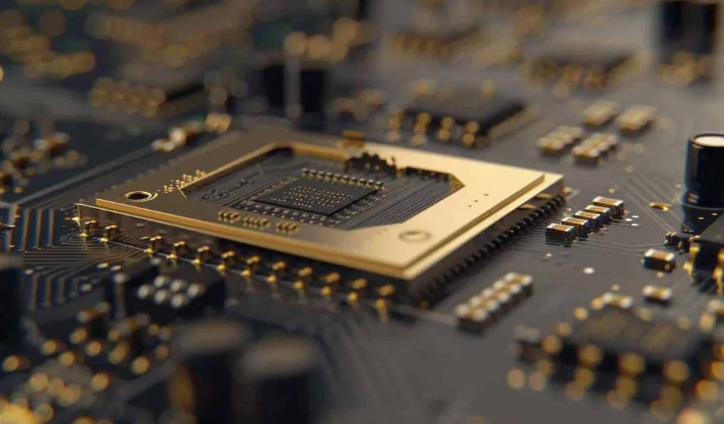
Designing a multilayer Printed Circuit Board (PCB) is a crucial skill for modern electronics, enabling compact, high-performance devices by stacking conductive and insulating layers. A successful multilayer PCB design hinges on a meticulously planned layer stackup, which dictates signal integrity, power distribution, and electromagnetic compatibility. This process involves defining layer functions, selecting appropriate materials like FR-4 or high-frequency laminates, and strategically routing traces to minimize noise and impedance mismatches, ensuring a reliable and manufacturable final product.
Mastering Multilayer PCB Design: A Comprehensive Guide
As electronic devices become smaller, faster, and more complex, the single or double-sided PCB often falls short. This is where multilayer PCBs come in. By incorporating additional layers, engineers can achieve higher component density, superior signal integrity, and effective power management. However, this complexity introduces new design challenges. This guide will walk you through the entire process, from conceptualizing the layer stackup to final manufacturability checks, empowering you to create robust and efficient multilayer designs.
Table of Contents
- What is a Multilayer PCB and Why Do You Need One?
- The Foundation of Success: Understanding the Multilayer PCB Stackup
- A Step-by-Step Guide to Designing Your Multilayer PCB
- Advanced Considerations for High-Performance Designs
- Design for Manufacturability (DFM) Best Practices
- Common Pitfalls in Multilayer PCB Design and How to Avoid Them
- Conclusion: Key Takeaways for a Successful Multilayer Design
- Frequently Asked Questions (FAQ)
What is a Multilayer PCB and Why Do You Need One?
A multilayer PCB is a printed circuit board that consists of more than two conductive copper layers. These layers are laminated together with insulating materials (known as *prepreg* and *core*) to form a single, unified board. While a double-sided board has a top and bottom layer, a multilayer board sandwiches one or more double-sided boards together, creating internal layers for routing and power distribution. This structure is the key to unlocking significant performance advantages.
The primary motivation for using a multilayer design is driven by necessity. You should consider moving to a multilayer PCB when:
- Component Density is High: When you’re using fine-pitch components like Ball Grid Arrays (BGAs) and there isn’t enough space on the outer layers to route all the necessary connections.
- High-Speed Signals are Present: Multilayer boards allow you to create controlled impedance traces and provide dedicated ground planes, which are essential for maintaining signal integrity and preventing data corruption in high-speed digital circuits.
- EMI/EMC is a Concern: The use of internal ground and power planes provides excellent shielding, reducing electromagnetic interference (EMI) emissions and improving the board’s susceptibility to external noise (EMC).
- Power Distribution is Complex: Dedicated power planes provide a low-inductance, stable voltage source for components, improving power integrity and reducing noise across the board.
The Foundation of Success: Understanding the Multilayer PCB Stackup
The single most important aspect of a multilayer PCB design is the layer stackup. It is the arrangement of copper layers and insulating layers that make up the board. Getting the stackup wrong can lead to a cascade of problems related to signal integrity, manufacturability, and cost, even if the rest of the layout is perfect. It should be the very first thing you define in your design process.
What Exactly is a PCB Layer Stackup?
The stackup is a detailed blueprint of the board’s cross-section. It defines the order of the layers, the thickness of each copper and dielectric layer, and the type of material used. A typical stackup consists of two main types of materials:
- Core: A rigid piece of dielectric material (like FR-4) with copper foil pre-bonded to one or both sides.
- Prepreg: A “pre-impregnated” sheet of fiberglass cloth with resin. It’s flexible until heated, at which point it melts and bonds the cores and copper foils together.
These materials are stacked in an alternating fashion—for example, Core / Prepreg / Foil—and then laminated under high temperature and pressure to create the final PCB.
Why is the Stackup So Critical for Performance?
A well-designed stackup is not just about fitting more traces; it’s a performance-critical engineering decision. It directly influences:
- Signal Integrity (SI): The thickness of the dielectric material between a signal layer and its reference plane (usually ground) determines the trace’s *characteristic impedance*. A consistent impedance is vital for preventing signal reflections and preserving data quality in high-speed circuits.
- Power Integrity (PI): Placing power and ground planes close together creates a natural, high-frequency decoupling capacitor, which helps provide stable power to integrated circuits.
- Electromagnetic Compatibility (EMC): Solid ground planes act as shields, containing electromagnetic fields from high-speed signals and preventing them from radiating outwards. Symmetrical stackups also prevent the board from warping during manufacturing.
Common Stackup Configurations and Their Applications
The number of layers you choose depends on the complexity of your design. Here are some common configurations and their typical uses:
| Number of Layers | Typical Stackup | Best For | Notes |
|---|---|---|---|
| 4-Layer | Signal | Ground | Power | Signal | General-purpose designs, good EMI performance, cost-effective upgrade from 2-layer. | The most common multilayer configuration. Placing ground and power planes internally provides excellent shielding. |
| 6-Layer | Signal | Ground | Signal | Signal | Power | Signal | High-speed designs with multiple signal busses (e.g., DDR memory). | Provides two internal signal layers for routing high-speed differential pairs, shielded by the adjacent ground/power planes. |
| 8-Layer | Signal | Ground | Signal | Power | Ground | Signal | Power | Signal | Complex, high-density designs with multiple power rails and high-speed interfaces. | Offers multiple ground planes for excellent EMI control and return path management, plus additional routing and power layers. |

A Step-by-Step Guide to Designing Your Multilayer PCB
With a solid understanding of the stackup, we can now move through the practical design process. Following these steps in order will help ensure a logical workflow and prevent costly mistakes.
Step 1: Defining Requirements and Selecting Materials
Before you draw a single trace, define the board’s electrical and physical requirements. What is the maximum signal frequency? What are the impedance requirements for critical traces (e.g., 50-ohm single-ended, 100-ohm differential)? The answers will guide your material selection. While FR-4 is the industry standard due to its low cost and good performance, high-frequency designs (above 1 GHz) may require specialized laminates with a lower *dielectric constant (Dk)* and *loss tangent (Df)* to minimize signal loss.
Step 2: Creating the Layer Stackup in Your CAD Tool
Using the requirements from Step 1, build the layer stackup in your PCB design software. Do not use the software’s default stackup. Instead, consult your chosen fabrication house. They can provide a proven, manufacturable stackup using materials they keep in stock. This collaboration is key to achieving your desired impedance values and avoiding production delays. Specify the function of each layer (e.g., “Top Signal,” “Internal Ground,” “Internal Power”).
Step 3: Strategic Component Placement
Component placement is a critical step that influences routability and thermal performance. Group related components together, such as placing decoupling capacitors as close as possible to the IC power pins they serve. Keep analog and digital sections separate to prevent digital noise from interfering with sensitive analog signals. Ensure high-power components have adequate copper planes for heat dissipation and are positioned for good airflow if required.
Step 4: Designing Power and Ground Planes
One of the primary advantages of a multilayer board is the ability to use solid planes for power and ground. A solid ground plane provides a continuous, low-inductance return path for signals, which is fundamental to good signal integrity and EMI control. Power planes ensure stable voltage delivery across the board. For boards with multiple voltage rails, you may need to create “split planes,” but be careful not to route a high-speed signal across the split, as this creates a gap in the return path and can cause significant EMI problems.
Step 5: Routing High-Speed and Critical Signals
Route the most critical signals first. This includes high-speed signals (like USB, Ethernet, DDR), clock lines, and sensitive analog signals.
- Use an impedance calculator to determine the correct trace width for your target impedance based on your layer stackup.
- Route high-speed differential pairs together and keep their lengths matched.
- Use adjacent ground planes as a reference for these signals.
- Whenever possible, route signal layers orthogonally (e.g., one layer horizontal, the next vertical) to minimize crosstalk between adjacent layers.
After critical nets are routed, you can proceed with routing the less critical, lower-speed signals.
Step 6: Mastering Via Design and Implementation
Vias are plated holes that connect different layers of the PCB. While essential, they are discontinuities that can degrade signal integrity if not managed properly.
- Through-hole Vias: Go through the entire board. They are the simplest and cheapest but can create stubs on unused layers.
- Blind Vias: Connect an outer layer to an inner layer without passing through the whole board.
- Buried Vias: Connect two or more inner layers without reaching an outer layer.
For high-speed signals, it’s crucial to place a ground-stitching via near the signal via whenever it changes its reference plane. This provides a short path for the return current to follow the signal, preventing it from spreading and causing EMI.
Advanced Considerations for High-Performance Designs
For cutting-edge designs, simply connecting the dots isn’t enough. You must actively manage the physics of high-speed electronics.
Ensuring Signal Integrity (SI)
Signal Integrity is the measure of the quality of an electrical signal. In multilayer PCBs, key SI concerns are:
- Impedance Control: Maintaining a consistent characteristic impedance along the entire trace length to prevent signal reflections.
- Crosstalk: Unwanted coupling between adjacent traces. Mitigate this by increasing the spacing between traces and ensuring a solid ground reference plane.
- Timing and Skew: Ensuring that related signals (like in a data bus) arrive at their destination at the same time. This is managed by length-matching the traces.
Managing Power Integrity (PI)
Power Integrity ensures that all components receive clean, stable power. This is achieved by using solid power and ground planes to create a low-impedance power distribution network (PDN). Strategic placement of decoupling capacitors near IC power pins is essential to supply instantaneous current demands and filter out high-frequency noise.
Mitigating EMI and EMC Issues
Proper multilayer design is your best defense against electromagnetic interference. The core principles are:
- Use unbroken ground planes directly adjacent to high-speed signal layers.
- Ensure every signal has a clear, short return path on the reference plane.
- Keep high-frequency loops (e.g., signal and its return path) as small as possible.
- Consider adding shielding cans around particularly noisy components like switching regulators or RF modules.
Design for Manufacturability (DFM) Best Practices
A brilliant design is useless if it cannot be manufactured reliably and affordably. Always design with the fabrication process in mind.
- Communicate Early: Talk to your fabrication house *before* you finalize your design to understand their capabilities (e.g., minimum trace/space, via sizes, supported materials).
- Check Annular Rings: Ensure the copper pad around a drilled via (the annular ring) is large enough to allow for manufacturing tolerances without breaking the connection.
- Use Standard Drill Sizes: Sticking to standard drill sizes can reduce cost.
- Symmetrical Stackup: Always design a symmetrical stackup (e.g., layer 1 is the same thickness as layer 8, layer 2 as 7, etc.) to prevent the board from warping during the high-temperature lamination process.
Common Pitfalls in Multilayer PCB Design and How to Avoid Them
- Ignoring the Stackup: The most common error. Define it first, in collaboration with your fabricator.
- Routing Over a Split Plane: Creating a massive gap in the signal’s return current path. This is a major source of EMI.
- Forgetting Return Path Vias: When a high-speed signal changes layers, its return current also needs a path. Add a nearby ground via.
- Inadequate Decoupling: Placing decoupling capacitors too far from the IC pins or connecting them with long, thin traces negates their effectiveness.
- Violating DFM Rules: Using clearances or trace widths that are too small for your manufacturer’s process, leading to low yield and high costs.
Conclusion: Key Takeaways for a Successful Multilayer Design
Designing a high-performance multilayer PCB is a systematic process rooted in a strong understanding of fundamental electrical principles. The key is to prioritize the layer stackup as the foundation of your entire design. By carefully planning your stackup, strategically placing components, managing signal and power integrity, and designing for manufacturability, you can harness the full power of multilayer technology. Always remember to collaborate with your fabrication house early and often to ensure your design is not only functional but also reliable and cost-effective to produce.
Frequently Asked Questions (FAQ)
How do I choose the number of layers for my PCB?
Start with a 4-layer board if you need good EMI performance or have moderate routing density. Increase to 6 or 8 layers if you have high-speed interfaces like DDR memory, multiple BGA components, or require several different power rails that would necessitate splitting planes.
What is the difference between a core and prepreg?
A core is a rigid piece of dielectric material with copper already laminated to it. Prepreg is a more flexible resin-impregnated cloth that is used to glue the cores and copper foils together during the lamination process. The thickness and type of these materials are critical for achieving target impedance.
Why is a solid ground plane so important?
A solid ground plane provides a continuous, low-impedance path for signal return currents. This minimizes the loop area of signals (reducing EMI), provides a stable reference for controlled impedance traces, and helps shield signals from external noise.
multilayer pcb design, pcb design guide, layer stackup, pcb layer stackup design, how to design multilayer pcb, 4-layer pcb design, signal integrity, pcb design rules, power integrity, pcb via design, design for manufacturability, pcb materials, FR-4, controlled impedance, EMI mitigation pcb