Introduction to EMI and Multilayer PCBs
In the rapidly evolving landscape of electronic design, electromagnetic interference (EMI) represents a critical challenge, particularly for *multilayer printed circuit board (PCB) designs*. EMI refers to any unwanted electromagnetic energy that can disrupt the operation of an electronic device, often manifesting as noise, degraded signal quality, or even complete system failure. As electronic devices become more compact, complex, and operate at higher frequencies, the propensity for EMI generation and susceptibility significantly increases. Multilayer PCBs, while offering unparalleled density and performance, introduce complex electromagnetic environments where signals, power, and ground interact across multiple planes, making EMI mitigation a nuanced and essential aspect of the design process. Understanding the sources of EMI and its propagation mechanisms is the first step toward developing effective prevention strategies.
The imperative to control EMI extends beyond merely ensuring functionality; it is also a matter of regulatory compliance. Government agencies worldwide mandate specific limits on electromagnetic emissions (EMC) from electronic devices to prevent interference with other equipment and to safeguard public health. Therefore, incorporating EMI reduction techniques from the *initial concept and design phase* of a multilayer PCB is not an optional add-on but a fundamental requirement for successful product development. This article will explore a systematic approach to minimizing EMI, focusing on practical design techniques applicable to various multilayer PCB configurations.
Why Multilayer PCBs are Susceptible to EMI (And Why We Use Them)
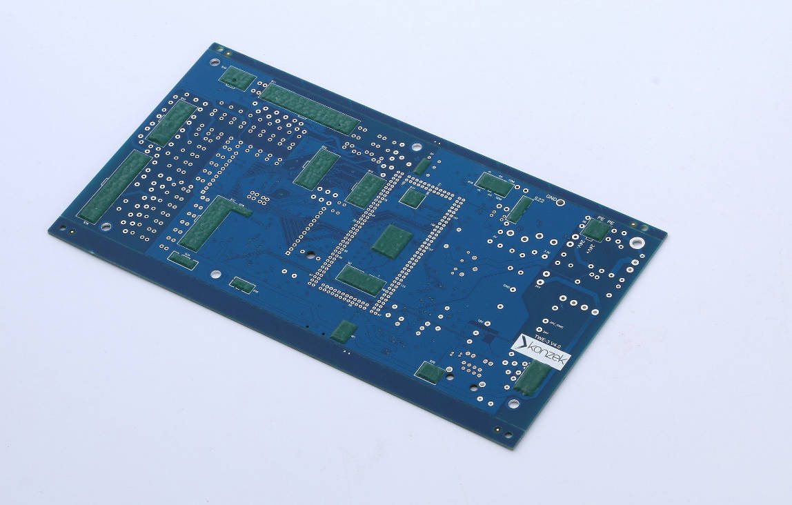
Multilayer PCBs are the backbone of modern electronics, enabling intricate designs with high component density and superior electrical performance compared to single or double-sided boards. Their construction involves multiple layers of conductive traces separated by insulating dielectric materials, offering dedicated planes for signals, power, and ground. This architecture facilitates shorter trace lengths, better impedance control, and enhanced signal integrity, which are crucial for high-speed digital and high-frequency analog circuits.
However, this very complexity also amplifies EMI challenges. The close proximity of signal, power, and ground layers creates numerous opportunities for capacitive and inductive coupling. High-speed signals transitioning between layers via vias can disrupt ground and power planes, creating impedance discontinuities and radiating noise. Furthermore, the numerous active components, each generating its own electromagnetic field, contribute to a dense electromagnetic environment where noise can easily propagate through conduction and radiation. Despite these challenges, the advantages of multilayer PCBs—including reduced board size, improved signal integrity, and the ability to manage complex power delivery networks—make them indispensable. Therefore, the focus shifts from avoiding EMI to intelligently managing and mitigating it within these sophisticated structures.
Fundamental Principles of EMI Control in PCB Design
Effective EMI control in multilayer PCB design is rooted in a few fundamental electromagnetic principles: *containment, isolation, and impedance control*. Containment aims to restrict electromagnetic fields to their intended paths and prevent them from radiating or coupling to other circuits. This often involves using ground planes as shields and ensuring complete return paths for current.
Isolation focuses on separating noise-generating circuits from noise-sensitive circuits, both physically and electrically. This can be achieved through strategic component placement, guard traces, and dedicated ground islands for sensitive analog sections. Impedance control is crucial, especially for high-speed signals, to prevent reflections and minimize radiation. By maintaining a consistent characteristic impedance along transmission lines and managing the impedance of power delivery networks, designers can significantly reduce EMI.
These principles guide virtually every design decision aimed at EMI mitigation. A proactive approach, integrating these considerations from the conceptual stage, is far more effective and cost-efficient than attempting to fix EMI problems after the PCB has been fabricated. Early attention to detail in layer stackup, component placement, and routing can prevent costly redesigns and delays in product launch.
Optimizing Layer Stackup for EMI Reduction
The layer stackup is arguably the most critical decision in multilayer PCB design, profoundly impacting signal integrity, power integrity, and, consequently, EMI performance. A well-planned stackup forms the foundation for EMI control by providing clear current return paths, effective shielding, and stable power distribution.
Basic Principles of Layer Stackup
At its core, an optimal layer stackup aims to create a low-impedance path for return currents directly beneath the signal traces. This minimizes the loop area formed by the signal and its return current, thereby reducing radiated emissions. The proximity of a signal layer to its adjacent reference plane (ground or power) is paramount. The tighter the coupling (i.e., the thinner the dielectric between them), the lower the loop inductance and the better the EMI performance. Conversely, poorly planned stackups can lead to excessive ground bounce, crosstalk, and broadside coupling, all of which contribute significantly to EMI.
Designers must consider the number of layers required based on design complexity, signal speeds, and density. While more layers offer greater flexibility for dedicated planes and shielding, they also increase cost and manufacturing complexity. A balanced approach is crucial, prioritizing EMI performance within budget and physical constraints. For instance, high-speed signals should always be routed on layers immediately adjacent to a solid reference plane.
Impact on Signal and Power Integrity
The chosen layer stackup directly influences both signal integrity (SI) and power integrity (PI), which are intrinsically linked to EMI. Good SI, characterized by minimal reflections, crosstalk, and ringing, inherently reduces EMI because signals propagate cleanly without generating unwanted noise. A solid reference plane provides a consistent characteristic impedance for traces and effectively shields them from external noise and vice versa.
Similarly, robust PI ensures a stable and clean power supply to all components. A well-designed power distribution network (PDN), facilitated by appropriate plane placement and effective decoupling, minimizes voltage fluctuations (ground bounce and Vcc bounce) that can inject noise into signal paths and radiate EMI. A noisy power plane can act as a radiating antenna, spreading EMI across the board. Therefore, a stackup that supports both excellent SI and PI simultaneously contributes significantly to overall EMI reduction.
Common Stackup Configurations and Their EMI Characteristics
Various stackup configurations exist, each with specific advantages and disadvantages regarding EMI. The choice often depends on the design’s complexity and budget. Here are some common examples:
- 4-Layer Stackup (Sig-GND-PWR-Sig): This is a cost-effective choice for moderately complex designs. The two outer signal layers can be referenced to inner planes. However, the proximity of PWR and GND planes can lead to broadside coupling if not managed carefully. Ideally, signals on the top layer reference GND, and signals on the bottom layer reference PWR.
- 4-Layer Stackup (Sig-GND-GND-Sig): This configuration provides two dedicated ground planes. While offering excellent shielding and return paths for signals on the outer layers, it lacks a dedicated power plane, making PDN design more challenging and potentially necessitating more power traces or islands. The two ground planes also offer an excellent low-impedance path for high-frequency return currents when stitched together with vias.
- 6-Layer Stackup (Sig-GND-Sig-PWR-GND-Sig): A popular choice for high-speed designs. It offers multiple signal layers with adjacent reference planes (GND, PWR) and provides a good level of isolation. The inner signal layers are sandwiched between reference planes, offering good shielding and controlled impedance.
- 8-Layer Stackup (Sig-GND-Sig-PWR-GND-Sig-GND-Sig): For very high-speed or high-density designs, an 8-layer stackup can provide excellent EMI performance. It allows for multiple dedicated signal, power, and ground planes, enabling tighter coupling and better isolation between different types of signals. Critical high-speed signals can be routed on buried layers, shielded by adjacent ground planes.
The table below summarizes the characteristics of common stackups:
| Stackup Type | Pros for EMI | Cons for EMI | Best Use Cases |
|---|---|---|---|
| 4-Layer (Sig-GND-PWR-Sig) | Cost-effective, reasonable signal integrity | Potential broadside coupling between PWR/GND, outer signals less shielded | Moderate speed, low-density designs |
| 4-Layer (Sig-GND-GND-Sig) | Excellent ground reference, good shielding for outer signals | No dedicated power plane, complex PDN design | Analog circuits, designs needing robust grounding |
| 6-Layer (Sig-GND-Sig-PWR-GND-Sig) | Multiple signal layers with adjacent planes, good isolation, controlled impedance | Increased cost/complexity | High-speed digital, mixed-signal designs |
| 8-Layer (Sig-GND-Sig-PWR-GND-Sig-GND-Sig) | Superior shielding, multiple dedicated planes, excellent SI/PI | Highest cost/complexity | Very high-speed, high-density, RF designs |
Strategic Placement of Ground and Power Planes
The strategic placement of ground and power planes is paramount. General guidelines include:
- Adjacent Reference Planes: Every signal layer, especially high-speed ones, should be immediately adjacent to a solid ground or power plane. This creates a well-defined return path and controlled impedance.
- Solid Ground Planes: Prioritize solid ground planes. Split ground planes should be avoided unless absolutely necessary for specific analog/digital isolation, and even then, careful bridging or filtering is required. Splits can force return currents to take long, inductive paths, creating radiating loops.
- Power and Ground Plane Proximity: Power and ground planes should be closely coupled (placed very close together) to form a low-impedance bypass capacitor, effectively reducing power supply noise.
- High-Speed Signal Layers: High-speed signals are best routed between two reference planes (e.g., between two ground planes, or between a ground and a power plane). This provides shielding from the outside world and reduces broadside coupling.
For example, in a 6-layer stackup, a common and effective configuration places ground planes on layers 2 and 5, with power on layer 4. Signal layers 1 and 6 can then reference layer 2 and 5 respectively, while signal layer 3 is sandwiched between two ground planes, offering excellent shielding. The close proximity of PWR (layer 4) to GND (layer 5) forms a parasitic capacitor, improving power integrity. Careful planning of the dielectric thickness between these planes is crucial for optimal performance.
Robust Power and Ground Plane Design for Noise Suppression
Beyond the stackup, the design of the power distribution network (PDN) and ground planes is a cornerstone of EMI mitigation. A robust PDN provides a stable voltage rail across the entire board, while an effective ground system serves as the common reference and return path for all currents.
The Importance of Solid Ground Planes
A solid ground plane is the single most effective EMI reduction technique. It provides a low-impedance, continuous return path for all signal currents, minimizing loop areas and thus reducing radiated emissions. Any breaks, slots, or perforations in the ground plane, especially under high-speed traces, can force return currents to divert, creating large inductive loops that act as efficient radiating antennas. This phenomenon, known as “ground plane discontinuity,” is a major source of EMI.
While via holes are unavoidable, they should be evenly distributed and kept as small as practical to maintain ground plane integrity. When it is absolutely necessary to route a trace through a ground plane (e.g., for components like connectors), the trace should be as short as possible and ideally bridged with stitching vias to maintain continuous ground on either side. For components with high-frequency currents, ensuring an uninterrupted ground plane directly beneath them is paramount.
Optimizing Power Delivery Networks (PDNs)
The power delivery network (PDN) is responsible for supplying stable, low-noise power to all active components. A poorly designed PDN can lead to voltage droop, ground bounce, and significant power supply noise, which directly translates to EMI. Key aspects of PDN optimization include:
- Low Impedance: The PDN should present a very low impedance across a wide frequency range to quickly deliver current transients demanded by switching components and suppress noise. This is achieved through closely coupled power and ground planes, and effective decoupling.
- Current Distribution: Power planes should be designed to distribute current evenly, avoiding bottlenecks or high-resistance paths. Wider power traces or planes are generally better.
- Minimizing Inductance: Loop inductance in the PDN contributes to noise. Keep power and ground planes close together, use multiple power pins on ICs, and place decoupling capacitors as close as possible to the IC power pins.
Tools for power integrity analysis (PI analysis) can simulate the PDN impedance and identify potential hotspots or resonant frequencies before fabrication, helping optimize plane shapes and decoupling strategies.
Effective Decoupling and Bypass Capacitors
Decoupling and bypass capacitors are fundamental to a low-impedance PDN and critical for EMI reduction. They act as local reservoirs of charge, supplying instantaneous current demanded by switching ICs and shunting high-frequency noise from power rails to ground.
- Placement: Capacitors must be placed as close as possible to the power pins of the ICs they serve. The loop inductance between the capacitor, the IC power pin, and the ground plane should be minimized. This usually means placing them on the same side of the PCB as the IC, directly next to the power pin, with short traces to the power and ground planes.
- Value and Type: A combination of different capacitor values (e.g., 0.1µF, 0.01µF, 1000pF) is often needed to cover a broad spectrum of frequencies. Ceramic capacitors (X7R, X5R, C0G) are preferred for high-frequency decoupling due to their low equivalent series inductance (ESL) and equivalent series resistance (ESR). Bulk capacitors (electrolytic, tantalum) handle lower-frequency demands and larger current swings.
- Via Placement: Vias connecting decoupling capacitors to the power/ground planes should be numerous, short, and directly under the capacitor pads to minimize inductance.
The goal is to create a very low impedance path from the IC to the capacitors, and then to the planes, ensuring that transient currents are supplied locally without drawing current from distant parts of the PDN, which could cause voltage drops and generate noise.
Grounding Techniques: Star Ground vs. Ground Plane
While a solid ground plane is generally preferred for multilayer PCBs due to its low impedance and excellent shielding, designers sometimes encounter situations where specialized grounding techniques are considered, such as *star grounding* for sensitive analog sections or mixed-signal designs. In a star ground system, all grounds converge at a single point to prevent ground loops and common-mode noise. However, implementing a true star ground on a complex multilayer PCB with high-speed digital signals is often impractical and can lead to its own set of EMI issues if return paths are elongated.
For most multilayer designs, a solid, contiguous ground plane acts as an inherently effective star ground at low frequencies, as all points are nominally at the same potential. For mixed-signal designs, it’s common to have a single, unified ground plane but to separate sensitive analog components and their return currents from noisy digital sections through strategic layout, component placement, and perhaps careful partitioning of their respective power supplies, ensuring their ground pins all connect to the same solid ground plane.
When split ground planes are unavoidable (e.g., for very sensitive analog isolation), they should only be used if signal return currents *never* cross the gap. If a signal trace must cross a ground split, it must be bridged by a capacitor or by routing the signal and its return path together across a single, narrow bridge, otherwise, it will create a large radiating loop.
Advanced Trace Routing Techniques to Minimize EMI
Once the layer stackup and PDN are established, the meticulous routing of individual traces becomes paramount for controlling EMI. Poor routing can negate the benefits of an optimized stackup and robust power planes.
Ensuring Clear Return Current Paths
Every current flowing through a signal trace must have a corresponding return current flowing in the opposite direction. For high-frequency signals, this return current tends to follow the path of least impedance, which is usually directly beneath the signal trace on the nearest reference plane. Discontinuities in this return path (e.g., a slot in the ground plane, a change of reference plane without proper via stitching) force the return current to diverge, creating a large loop area that acts as an efficient antenna, radiating EMI. The larger the loop area, the greater the inductance and the higher the radiated emissions.
Therefore, designers must ensure an uninterrupted return path directly adjacent to all signal traces, especially high-speed ones. When a signal trace changes layers, its return current must also have an immediate path to change layers. This is typically achieved using “stitching vias” placed adjacent to the signal via, connecting the old reference plane to the new one, ensuring the return current maintains a tight loop.
Routing Differential Pairs for EMI Immunity
Differential pairs, commonly used for high-speed interfaces like USB, HDMI, and Ethernet, are inherently robust against common-mode noise and generally emit less EMI than single-ended signals. However, their EMI performance depends heavily on proper routing:
- Tight Coupling: The two traces in a differential pair should be routed as closely and parallel as possible to maintain tight magnetic coupling. This ensures that any induced noise appears as common-mode and is rejected by the differential receiver.
- Length Matching: Maintain precise length matching between the two traces to prevent skew, which can convert differential-mode signals into common-mode noise.
- Impedance Control: Ensure controlled differential impedance throughout the trace length.
- Continuous Reference Plane: Route differential pairs over a continuous, solid reference plane to provide a consistent return path and minimize emissions. Avoid routing over splits or voids in planes.
- Minimize Vias: Avoid using vias in differential pairs whenever possible, as they introduce impedance discontinuities. If vias are unavoidable, ensure both traces have matching via structures and use adjacent ground stitching vias.
The goal is to preserve the common-mode rejection properties of the differential signaling, which effectively cancels out much of the radiated EMI.
Controlled Impedance Routing
Controlled impedance routing is essential for high-speed signals to prevent reflections that can cause ringing, overshoot, undershoot, and signal degradation. These signal integrity issues are often significant sources of EMI. By matching the trace impedance to the source and load impedances, reflections are minimized, ensuring clean signal transitions. This typically involves calculating trace width, dielectric thickness, and trace-to-plane spacing based on the material properties of the PCB.
Maintaining a consistent characteristic impedance along the entire length of the transmission line, including through vias and connectors, is crucial. Any abrupt changes in impedance will lead to reflections and potential EMI. Tools like field solvers and stackup calculators are indispensable for accurate impedance control.
Trace Spacing and Crosstalk Mitigation
Trace spacing plays a vital role in mitigating crosstalk, which is the unwanted coupling of electromagnetic energy between adjacent traces. Crosstalk can be a significant source of EMI, as noise from one trace can induce unwanted signals in another. To minimize crosstalk:
- Rule of 3W: A common guideline states that the spacing between adjacent high-speed traces should be at least three times the trace width (3W). This increases the coupling loss between traces, reducing both inductive and capacitive crosstalk.
- Separation of Signal Types: Separate high-speed digital signals from low-speed analog signals, clock lines from data lines, and noisy traces from sensitive ones. Dedicated routing channels or layers can be beneficial.
- Guard Traces: For extremely sensitive signals or noisy traces, guard traces (grounded traces routed parallel to the signal trace) can be used to provide additional shielding and sink induced noise. These guard traces should be periodically stitched to the ground plane.
The goal is to prevent unintended energy transfer between traces, keeping signals clean and reducing radiated noise.
Via Selection and Placement Strategies
Vias are necessary for connecting traces between different layers, but they introduce parasitic inductance and capacitance, creating impedance discontinuities that can degrade signal integrity and generate EMI, especially at high frequencies. Strategies for managing vias include:
- Minimize Vias: Reduce the number of vias in high-speed signal paths as much as possible.
- Via Size: Use smaller via barrels and antipads to minimize their parasitic capacitance and inductance.
- Blind/Buried Vias: For very high-speed or dense designs, blind and buried vias can be beneficial. They only pass through necessary layers, reducing stub length and associated reflections and EMI. Through-hole vias that pass through many unused layers create stubs that can resonate and cause significant signal integrity and EMI issues.
- Stitching Vias: As mentioned, use stitching vias when signal traces change reference planes to provide a continuous, low-impedance return path. These should be placed immediately adjacent to the signal via.
Careful via management is crucial for maintaining signal integrity and minimizing potential EMI hotspots.
Utilizing Guard Traces and Stitching Vias
Guard traces, also known as shielding traces, are unrouted copper traces connected to ground and placed parallel to sensitive or noisy signal traces. They act as a barrier, intercepting electromagnetic fields and shunting induced noise to the ground plane, thereby reducing crosstalk and direct radiation. For maximum effectiveness, guard traces should be stitched to the ground plane with vias at regular intervals (e.g., every 5-10 times the dielectric thickness) to ensure they are at a consistent ground potential along their entire length. Without proper stitching, a guard trace can itself act as an antenna.
Stitching vias are also essential for connecting adjacent ground planes or sections of a single ground plane across different layers, especially around cutouts or near high-frequency components. This ensures a robust, low-impedance ground reference across the entire board, preventing ground loops and providing effective shielding.
Strategic Component Placement for EMI Control
The physical arrangement of components on a multilayer PCB is just as critical as the routing and stackup in controlling EMI. Thoughtful component placement can minimize noise generation and susceptibility from the outset.
Identifying and Locating Critical Components
Begin by identifying critical components: those that are high-frequency noise sources (e.g., clock generators, switching power supplies, high-speed microcontrollers) and those that are highly susceptible to noise (e.g., analog-to-digital converters, low-noise amplifiers, sensitive sensors). These components require special attention regarding their placement and isolation.
High-speed components should be placed close to their connectors or interfaces to minimize trace lengths, thereby reducing the “antenna” size for radiated emissions. Group related components together (e.g., a microprocessor with its associated memory and power regulation) to keep high-frequency current loops small and contained within a localized area.
Separation of Noise Sources and Sensitive Circuitry
A fundamental principle is to physically separate noise-generating circuitry from noise-sensitive circuitry. This means placing digital sections away from analog sections, power sections away from RF sections, and high-current paths away from low-current signal paths. Where complete physical separation is not possible, barriers such as grounded guard rings or even dedicated ground plane splits (used with extreme caution and proper bridging) might be considered for extreme isolation of highly sensitive analog blocks.
For example, a switching power supply, a major EMI source, should be placed in a dedicated corner of the board, with its high-current loops kept as small as possible and its ground connections carefully managed to prevent noise injection into sensitive areas.
Placement of Filtering and Decoupling Components
The effectiveness of filtering and decoupling components (capacitors, ferrite beads, common-mode chokes) is highly dependent on their placement. Decoupling capacitors must be placed as close as possible to the power pins of the ICs they protect, as discussed earlier. Similarly, filtering components should be placed at the point of entry or exit of signals or power, to filter noise before it enters or leaves the sensitive circuitry.
For instance, ferrite beads used to filter power lines should be placed immediately after the power source and before the IC, with a decoupling capacitor on the IC side of the ferrite bead. This creates an effective low-pass filter. Common-mode chokes on data lines should be placed close to the connector or the point where signals transition off the board.
Incorporating Filtering and Shielding Measures
Even with optimal stackup, routing, and placement, some residual EMI may persist. Additional filtering and shielding measures can provide the necessary final reduction to meet EMI compliance targets.
On-Board Filtering Techniques (Ferrite Beads, Chokes)
On-board filtering components target specific frequency ranges of noise:
- Ferrite Beads: These act as lossy inductors at high frequencies, effectively attenuating high-frequency noise on power lines and signal lines. They are particularly useful for damping resonant peaks in the PDN or filtering common-mode noise. Placement is critical: they should be located at the point of entry/exit of noise, with proper bypassing capacitors on the filtered side.
- Common-Mode Chokes: These are effective in suppressing common-mode noise on differential signal pairs or power lines. They present a high impedance to common-mode currents while allowing differential currents to pass unimpeded. They are typically placed on I/O lines close to the connector or where cables attach.
- RC/LC Filters: Simple resistor-capacitor (RC) or inductor-capacitor (LC) low-pass filters can be implemented on sensitive analog power rails or signal lines to filter out high-frequency noise.
The choice and placement of these components require careful consideration of the noise frequencies present and the impedance characteristics of the circuit.
Enclosure and Internal Shielding Considerations
Beyond the PCB itself, the enclosure and internal shielding play a crucial role in EMI containment. A metallic enclosure can act as a Faraday cage, blocking both incoming and outgoing electromagnetic radiation. Key considerations for enclosure shielding include:
- Continuity: The enclosure must have electrical continuity across all its seams and joints to be an effective shield. Gaps can act as slots, allowing EMI to leak. Conductive gaskets or finger stock may be needed.
- Apertures: Any openings (for connectors, displays, ventilation) must be designed to minimize EMI leakage. Small holes or honeycomb structures can pass air while attenuating high-frequency fields.
- Grounding: The PCB should be properly grounded to the enclosure at a single point (or multiple points if necessary, with careful consideration) to prevent ground loops and to ensure the enclosure is at the same potential as the PCB ground reference.
- Internal Shielding: For highly sensitive or noisy sub-circuits, internal shielding cans or compartmentalization within the PCB enclosure can provide additional isolation. These shields must also be properly grounded.
Effective enclosure design complements on-board EMI reduction by providing the final barrier against electromagnetic interference.
Design Review, Simulation, and Verification for EMI Compliance
A rigorous process of design review, simulation, and verification is indispensable for ensuring EMI compliance. Catching potential issues early in the design cycle saves significant time and cost.
Utilizing Simulation Tools (SI/PI Analysis)
Modern electronic design automation (EDA) tools offer powerful Signal Integrity (SI) and Power Integrity (PI) analysis capabilities. These tools can:
- Pre-Layout Analysis: Simulate transmission line effects, impedance control, and power delivery network characteristics even before routing begins.
- Post-Layout Analysis: Analyze actual routed traces for reflections, crosstalk, and ground bounce.
- EMI/EMC Simulation: Some advanced tools can predict radiated and conducted emissions based on the layout, identifying potential hotspots and allowing for design adjustments.
- Thermal Analysis: While not directly EMI, thermal performance is often related to power consumption and can indirectly affect component stability, which can influence EMI.
By using these tools, designers can identify and correct potential EMI issues virtually, reducing the number of physical prototypes required and accelerating the design cycle.
Pre-compliance and Full Compliance EMI Testing
Despite best design practices and simulation, real-world EMI testing is the ultimate arbiter of compliance. Two main types of testing are relevant:
- Pre-compliance Testing: Conducted in-house or at a local lab, pre-compliance testing aims to identify major EMI issues early in the development cycle. It uses scaled-down versions of formal test setups and provides valuable feedback to inform design iterations before committing to expensive full compliance testing. This often involves spectrum analyzers, near-field probes, and an anechoic chamber or reverberation chamber.
- Full Compliance Testing: This is performed by accredited test laboratories according to specific regulatory standards (e.g., FCC Part 15, CISPR, CE). It involves rigorous testing for radiated emissions, conducted emissions, and immunity to various electromagnetic phenomena. Passing full compliance testing is mandatory for product certification and market entry.
It is far more cost-effective to identify and fix EMI problems during pre-compliance testing than to fail full compliance and necessitate costly redesigns.
EMI Design Checklists and Best Practices
Adhering to a comprehensive EMI design checklist throughout the design process can significantly improve the chances of first-pass success. Such a checklist typically covers:
- Layer stackup verification (number of layers, plane types, dielectric thickness).
- PDN impedance and decoupling capacitor placement.
- High-speed signal routing (return paths, impedance control, differential pair guidelines).
- Component placement (separation of noisy/sensitive circuits).
- Via management (stitching vias, blind/buried vias).
- Filtering (ferrite beads, common-mode chokes).
- Grounding scheme integrity.
- Enclosure and connector grounding.
Regular design reviews with EMI specialists or experienced PCB designers can also uncover potential pitfalls before they become costly problems.
Conclusion: A Holistic Approach to EMI Mitigation
Reducing EMI in multilayer PCB designs is a multifaceted challenge that demands a holistic and proactive approach. It’s not a single technique but a systematic integration of best practices across every stage of the design process, from initial concept to final verification. By meticulously planning the layer stackup, designing robust power and ground planes, employing advanced trace routing techniques, strategically placing components, and incorporating appropriate filtering and shielding, engineers can significantly mitigate EMI. The ultimate goal is to create PCBs that are not only functionally superior but also inherently resilient to electromagnetic interference, ensuring reliable performance and seamless compliance with global regulatory standards. Embracing a culture of “design for EMI” from the outset will lead to more efficient development cycles, reduced costs, and higher quality electronic products.