1. Introduction: The Imperative of Quality in Multilayer PCBs
This section will introduce the critical importance of quality control in the manufacturing of multilayer printed circuit boards (PCBs). It will highlight how multilayer PCBs, with their intricate designs and high component density, demand stringent quality measures to ensure reliability, performance, and longevity in diverse applications, from consumer electronics to aerospace. The featured snippet will be strategically placed here, emphasizing the comprehensive nature of QC.
Why Quality Control is Non-Negotiable in Multilayer PCBs
Explore the consequences of quality failures, including product recalls, system malfunctions, and reputational damage. Discuss the cost-benefit analysis of investing in robust QC processes, emphasizing how prevention is significantly more cost-effective than remediation. Use terms like _”reliability challenges,”_ _”defect prevention,”_ and _”performance assurance.”_
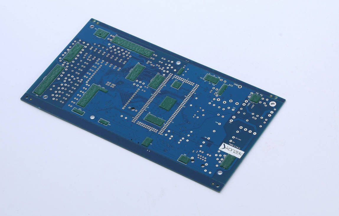
The Complexity Challenge: What Makes Multilayer PCBs Unique?
Detail the structural intricacies of multilayer PCBs, including multiple conductive layers, buried and blind vias, controlled impedance requirements, and fine line traces. Explain how these complexities amplify the potential for manufacturing defects compared to single or double-sided PCBs, making each production step a critical control point. Keywords: _”complex PCB structures,”_ _”interlayer registration
2. Foundational Pillars of Multilayer PCB Quality Assurance
Design for Manufacturability (DFM) and Design for Testability (DFT)
Discuss how early engagement in the design phase is crucial. DFM ensures the PCB layout can be reliably produced with minimal defects, considering trace widths, spacing, via sizes, and panel utilization. DFT incorporates features that facilitate efficient and accurate testing throughout the manufacturing process, such as test points and proper net accessibility. Keywords: _”optimizing PCB design,”_ _”reducing manufacturing defects,”_ _”test point implementation.”_
Material Selection and Incoming Material Inspection (IMI)
Elaborate on the importance of selecting high-grade raw materials that meet specified electrical, mechanical, and thermal properties. Detail the rigorous IMI process, which involves verifying material specifications against purchase orders and conducting physical and chemical tests to detect deviations before materials enter production. Use terms like _”raw material quality,”_ _”supplier qualification,”_ _”material verification.”_
_Substrates, Prepregs, and Copper Foils: What to Look For?_
Provide specific examples of critical material properties to inspect for each component: dielectric constant, dissipation factor, glass transition temperature (Tg) for substrates/prepregs, and copper purity, thickness, and surface roughness for foils. Discuss common defects like foreign inclusions or uneven coating.
_Chemical Purity and Storage Conditions_
Address the importance of chemical purity for etchants, plating solutions, and soldermask, as impurities can severely impact process yield and final product quality. Explain the necessity of proper storage conditions (temperature, humidity) for all materials to prevent degradation.
3. Key Quality Control Stages in Multilayer PCB Production
This section forms the core of the article, systematically detailing the QC processes applied at each major step of multilayer PCB manufacturing. It will provide an in-depth look at techniques and their specific objectives.
Inner Layer Imaging and Etching Quality
Focus on the precision required for the internal conductive patterns. Explain the critical role of accurate imaging and controlled etching to prevent shorts, opens, and impedance variations within the hidden layers. Keywords: _”inner layer defects,”_ _”trace integrity,”_ _”pattern fidelity.”_
_Photolithography Precision: Preventing Shorts and Opens_
Describe the photolithography process for creating circuit patterns. Detail how QC monitors for accurate artwork alignment, proper UV exposure, and resist adhesion to prevent pattern distortion, bridging (shorts), and missing traces (opens). Emphasize the use of high-resolution film or direct imaging systems.
_Etching Uniformity and Under-Etching/Over-Etching Detection_
Explain the chemical etching process. Discuss how QC ensures uniform etching across the panel, preventing _under-etching_ (resulting in wider traces, potential shorts) and _over-etching_ (resulting in thinner traces, potential opens or impedance issues). Techniques include visual inspection and etch factor measurements.
Automated Optical Inspection (AOI) and Automated X-ray Inspection (AXI)
These are crucial automated inspection methods. This subsection will differentiate their applications and explain their mechanisms for defect detection. Keywords: _”automated defect detection,”_ _”hidden defect identification,”_ _”non-destructive testing.”_
_How AOI Detects Surface Defects and Pattern Discrepancies_
Describe how AOI machines use high-resolution cameras to scan PCB surfaces, comparing images to a “golden reference” or design data. Detail the types of defects AOI can find: shorts, opens, incorrect trace widths, missing pads, and copper voids on outer layers or after inner layer imaging.
_AXI for Internal Voids, Misalignments, and Buried Features_
Explain the principle of AXI, which uses X-rays to penetrate the PCB and reveal internal structures that AOI cannot see. Focus on its ability to detect _inner layer misregistration_, _voids in vias_, _barrel cracks_, and other buried defects, especially critical for complex multilayer structures.
Lamination Process Control: Ensuring Integrity and Adhesion
The lamination stage is where individual layers are bonded together. This section will detail the critical controls to ensure structural integrity. Keywords: _”lamination defects,”_ _”interlayer bonding,”_ _”structural integrity.”_
_Temperature, Pressure, and Time Profiles: Critical Parameters_
Elaborate on the precise control required for lamination parameters. Explain how deviations in temperature, pressure, or curing time can lead to delamination, resin starvation, resin richness, or voids, compromising the PCB’s mechanical and electrical properties.
_Void Detection and Delamination Prevention Techniques_
Discuss methods like _ultrasonic scanning_ or _microsection analysis_ (post-lamination) to detect voids or areas of poor adhesion. Highlight process controls, such as proper material handling and pre-baking, to prevent moisture-induced defects during lamination.
Drilling and Plating Quality: Via Reliability
Vias are crucial for interlayer connectivity. This section will cover the QC for their formation and metallization. Keywords: _”via defects,”_ _”plated through hole quality,”_ _”interconnection reliability.”_
_Drill Registration and Aspect Ratio Challenges_
Explain the importance of accurate drill registration (hole placement) relative to inner layer pads. Discuss how QC checks for drill wander, broken drills, or incorrect drill sizes. Address challenges with high _aspect ratio_ vias and how QC monitors for proper drilling parameters.
_Electroless and Electrolytic Plating: Ensuring Uniform Copper Deposition_
Describe the two-step plating process. Detail how QC monitors bath chemistry, current density, and agitation to ensure uniform copper deposition on via walls and surface pads. Emphasize the prevention of _”knee voids,”_ _”dog bones,”_ or _”pull-aways”_ in the plating layer.
_Via Integrity Testing: Microsection Analysis and Electrical Continuity_
Explain how _microsectioning_ is used to visually inspect the cross-section of vias for defects like cracks, voids, resin recession, or insufficient plating thickness. Also, mention electrical tests to confirm continuity through vias.
Outer Layer Imaging and Soldermask Application
This covers the final pattern formation and protective coating. Keywords: _”surface pattern accuracy,”_ _”soldermask adhesion,”_ _”component assembly readiness.”_
_Alignment and Resolution for Fine Pitch Components_
Discuss the critical accuracy required for imaging the outer layers, especially for fine-pitch components, to ensure proper pad registration and prevent shorts or opens. QC checks for accurate registration, trace width, and spacing.
_Soldermask Adhesion and Thickness Uniformity_
Explain the role of soldermask in protecting copper traces and preventing solder bridging. Detail QC for proper soldermask thickness (to prevent _solder dams_ or _starvation_), adhesion (to prevent peeling during assembly), and accurate opening of pads.
Surface Finish Application and Final Quality Checks
The final protective layer and comprehensive inspection. Keywords: _”solderability,”_ _”environmental protection,”_ _”final inspection.”_
_ENIG, OSP, HASL: Ensuring Solderability and Environmental Resistance_
Discuss different surface finishes (e.g., Electroless Nickel Immersion Gold (ENIG), Organic Solderability Preservative (OSP), Hot Air Solder Leveling (HASL)). Detail QC for ensuring correct thickness, composition, and uniform coverage, which directly impacts solderability and shelf life. Mention _black pad_ prevention in ENIG.
_Contamination Control and Cleanliness Standards_
Emphasize the importance of maintaining a clean manufacturing environment and ensuring the final PCB is free from dust, debris, and chemical residues. Discuss ionic cleanliness testing (_Ion Chromatography_) and visual inspection for surface contaminants.
4. Advanced Testing and Inspection Methodologies
Electrical Testing: Continuity, Insulation Resistance, and Impedance Control
_Flying Probe vs. Fixture Testing: When to Use Which?_
Compare and contrast these two primary electrical test methods. Flying probe testing is flexible for prototypes and low-volume, while fixture (bed-of-nails) testing is efficient for high-volume production. Detail what each test checks for (opens, shorts, resistance values).
_Time Domain Reflectometry (TDR) for Controlled Impedance_
Elaborate on TDR’s role in verifying _controlled impedance_ lines. Explain how TDR measures impedance uniformity along specific traces, critical for high-speed digital and RF applications where signal integrity is paramount. Keywords: _”signal integrity testing,”_ _”impedance matching.”_
Microsection Analysis and Destructive Physical Analysis (DPA)
_Revealing Internal Structures and Identifying Hidden Defects_
Describe the process of microsectioning a PCB to visually inspect critical internal features such as via barrel quality, interlayer connections, plating thickness, and delamination. Highlight its role in root cause analysis for failed boards.
_IPC Standards: The Gold Standard for PCB Inspection_
Introduce IPC standards (e.g., IPC-A-600, IPC-6012) as the industry benchmarks for acceptability criteria in PCB manufacturing and inspection. Explain how manufacturers adhere to these standards for defect classification and quality assurance.
Thermal Stress and Environmental Testing
_Thermal Shock and Temperature Cycling for Reliability_
Explain these tests, where PCBs are subjected to rapid changes between extreme hot and cold temperatures to simulate operational stress. This helps identify weaknesses like cracked vias, delamination, or solder joint failures that might not appear at room temperature.
_Humidity and Moisture Resistance Assessments_
Detail how PCBs are tested under high humidity and elevated temperatures to assess their resistance to moisture absorption, which can lead to reduced insulation resistance, electrochemical migration, or material degradation.
5. Implementing a Robust Quality Management System (QMS)
ISO 9001 and IPC Standards: Frameworks for Excellence
Explain how adherence to international standards like ISO 9001 (quality management) and industry-specific standards from IPC (e.g., IPC-1791 for qualified manufacturers) establishes a foundation for consistent quality. Discuss the benefits of certification.
Traceability and Documentation: From Raw Material to Finished Product
Emphasize the importance of meticulous record-keeping for every stage of production, including batch numbers, process parameters, inspection results, and material origins. This allows for _root cause analysis_ and recall management if defects are discovered later. Keywords: _”full traceability,”_ _”quality records,”_ _”audit readiness.”_
Continuous Improvement and Root Cause Analysis (RCA)
Discuss the philosophy of continuous improvement (e.g., Six Sigma, Lean Manufacturing) in QC. Explain how RCA tools (e.g., Ishikawa diagrams, 5 Whys) are used to identify and address the fundamental causes of defects, preventing recurrence and enhancing overall process efficiency.
6. Challenges and Future Trends in Multilayer PCB Quality Control
Miniaturization and Ultra-Fine Pitch Challenges
Discuss how the relentless drive for smaller, denser PCBs with ultra-fine pitch features (e.g., µBGA, HDI) pushes the limits of current inspection technologies. Highlight the increasing difficulty in detecting minuscule defects and maintaining tight tolerances.
Advanced Materials and Heterogeneous Integration
Address the QC implications of new, high-performance materials (e.g., low-loss dielectrics, flexible substrates) and the integration of diverse technologies (e.g., embedded components, optical interconnects). These require specialized inspection techniques and material characterization.
AI and Machine Learning in QC: The Next Frontier
Explore the potential of AI and machine learning algorithms to revolutionize PCB inspection. Discuss applications in enhancing AOI/AXI capabilities, predicting potential defects based on process data, and automating defect classification, leading to faster, more accurate, and more intelligent QC.
7. Conclusion: The Enduring Value of Meticulous Quality Control
Summarize the overarching importance of comprehensive quality control throughout the entire multilayer PCB manufacturing process. Reiterate that a proactive, multi-faceted approach to quality not only ensures product performance and reliability but also drives innovation, reduces costs, and builds customer trust in a highly competitive industry. Emphasize that quality is not just a department but a culture.