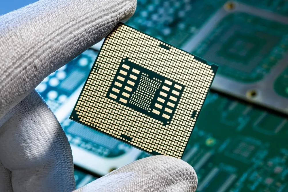
Integrated Circuit Substrate PCBs
The global integrated circuit shortage from 2020 to 2022 underscored the critical role of integrated circuits (ICs) in today’s electronics. The packaging of these ICs relies on specialized substrates, essential for ensuring strong connections to printed circuit boards (PCBs). Mars PCB provides expert PCB assembly services that support the creation of high-quality IC substrates, guaranteeing optimal performance for your electronic products.
This guide explores IC substrates in depth, focusing on their definition, classifications, applications, and, most importantly, their manufacturing processes. With a special emphasis on the evolution of manufacturing techniques from subtractive to advanced semi-additive methods, you’ll gain a comprehensive understanding of IC substrates by the end.
What is an IC Substrate?
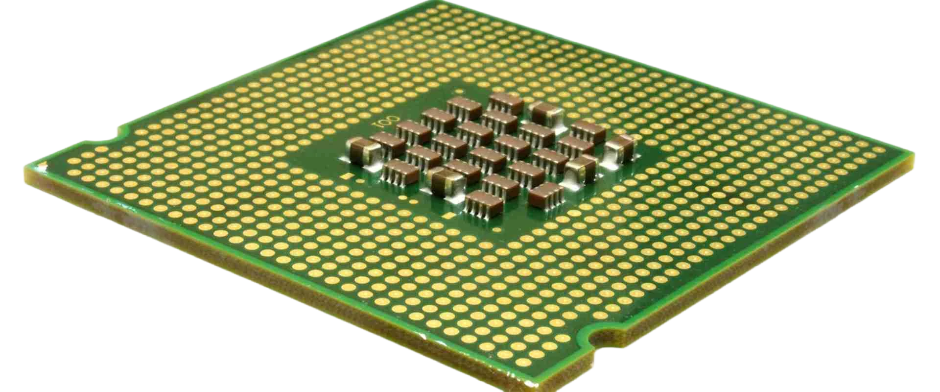
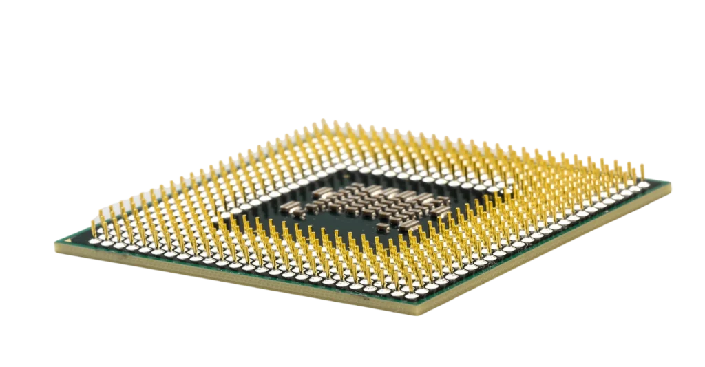
An integrated circuit substrate (IC package substrate) is the foundational material in IC packaging. It serves two primary purposes: protecting the bare IC and facilitating electrical connections between the IC and the PCB’s trace network. These connections significantly influence circuit performance.
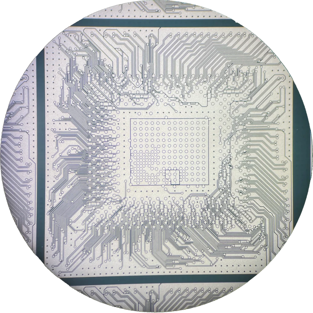
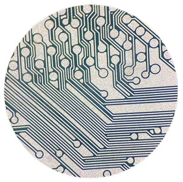
IC substrates consist of multiple layers built around a supporting core. They include a dense network of drilled holes and conductor pads, distinguishing them from standard PCBs and making their fabrication more complex.
Classifications of IC Substrate
IC substrates are classified based on package types, bonding technology, and material characteristics.
By Bonding Technology
Bonding technology defines how the IC connects to the package or external circuits:
- Wire Bonding: The most common method, using wires threaded from the chip to the package or external circuit.
- Tape Automated Bonding (TAB): Bonds the IC to fine conductors in a polymer-based substrate, creating flexible printed circuits (FPCs).
- Flip Chip (FC): Employs solder balls to connect chip pads to external circuit pads, secured with adhesives or solder interfaces.
By Package Types
The package type determines the substrate variety required:
- Ball Grid Array (BGA) IC Substrate: Suited for ICs with over 300 pins, offering excellent electrical performance and heat dissipation.
- Chip-Scale Package (CSP) IC Substrate: Thin and miniaturized, ideal for single-chip packages with fewer pins.
- Flip-Chip (FC) IC Substrate: Optimized for flip-chip connections, ensuring good heat dissipation and signal integrity.
- Multi-Chip Module (MCM) IC Substrate: Supports multiple ICs with diverse functions, requiring lightweight substrates that maintain signal and heat management.
By Material Characteristics
Substrate materials vary based on IC requirements:
- Rigid: Made from resin-based materials like Ajinomoto Build-up Film (ABF), Epoxy, or Bismaleimide Triazine (BT).
- Flex: Uses Polyimide or Polyamide resin, balancing electrical performance and thermal expansion.
- Ceramic: Composed of materials like aluminum nitride, silicon carbide, or aluminum oxide for high-performance applications.
Applications of IC Substrate PCBs
IC substrates are integral to:
- Memory Chip Packaging
- Micro-Electromechanical Systems (MEMS) Packaging
- Micro-Electromechanical Systems (MEMS) Packaging
- Processor Chip Packaging
- High-Speed Communication Device Packaging
These substrates are widely used in:
- Mobile Devices (smartphones, tablets)
- Mobile Devices (smartphones, tablets)
- Medical Devices
- Telecommunications
- Aerospace & Military Equipment
- Industrial Machinery
Characteristics of IC Substrates
IC substrates possess key attributes:
- Lightweight: Due to the materials used.
- Extremely Reliable: Solid materials protect the IC.
- Compact: Miniaturized design minimizes material usage.
- Durable: Robust despite their small footprint.
Manufacturing Technology of IC Substrates
The manufacturing of IC substrates has evolved significantly to meet the demands of modern electronics, particularly in terms of precision and miniaturization. Below, we detail the primary manufacturing processes, ordered from lower to higher precision: Subtractive Process (SP), Modified Semi-Additive Process (MSAP), Embedded Pattern Plating (EPP), and Semi-Additive Process (SAP).
Overview of Manufacturing Processes
The progression of these processes reflects the industry’s need for finer line widths, tighter spacing, and enhanced performance in high-density IC substrates. Each method builds on the previous one, offering greater precision and suitability for advanced applications.
Subtractive Process (SP)
Description: An improvement over SP, enabling finer features and higher precision.
Steps:
1.Electroplate a thin copper layer onto the substrate.
2.Apply a protective layer to define circuit patterns.
3.Plate additional copper onto exposed areas.
4.Remove excess copper via flash etching.
Precision: Achieves line widths of 20-30µm.
Applications: Widely used for modern IC substrates and high-density interconnect (HDI) designs.
Advantages: Balances cost and precision, making it a popular choice for many applications.
Modified Semi-Additive Process (MSAP)
Description: An improvement over SP, enabling finer features and higher precision.
Steps:
1.Electroplate a thin copper layer onto the substrate.
2.Apply a protective layer to define circuit patterns.
3.Plate additional copper onto exposed areas.
4.Remove excess copper via flash etching.
Precision: Achieves line widths of 20-30µm.
Applications: Widely used for modern IC substrates and high-density interconnect (HDI) designs.
Advantages: Balances cost and precision, making it a popular choice for many applications.
Embedded Pattern Plating (EPP)
Steps:
1.Apply a thin seed layer to the substrate.
2.Define circuit patterns using photolithography.
3.Plate copper into the defined patterns.
4.Remove the seed layer, leaving the plated patterns.
Precision: Achieves line widths of 10-15µm.
Applications: Ideal for advanced HDI substrates and high-density IC packaging.
Advantages: Provides greater control over feature size, supporting complex designs.
Semi-Additive Process (SAP)
Steps:
1.Use an insulating substrate with a photosensitive catalyst.
2.Selectively deposit copper using photolithography and plating techniques.
3.Form circuit patterns directly without etching.
Precision: Achieves line widths of 5-10µm.
Applications: Perfect for advanced IC substrates in high-speed communication devices and processor packaging.
Advantages: Offers unparalleled precision and efficiency for the most demanding applications.
Comparison of Manufacturing Processes
Process | Precision (Line Width) | Applications |
Subtractive (SP) | ~50µm | Standard PCBs, basic IC substrates |
MSAP | 20-30µm | Modern IC substrates, HDI |
EPP | 10-15µm | Advanced HDI, high-density IC substrates |
SAP | 5-10µm | Cutting-edge IC substrates, high-speed applications |
Key Manufacturing Steps
Regardless of the process, IC substrate manufacturing involves several critical steps:
- Lightweight: Due to the materials used.
- Extremely Reliable: Solid materials protect the IC.
- Extremely Reliable: Solid materials protect the IC.
- Compact: Miniaturized design minimizes material usage.
- Durable: Robust despite their small footprint.
Manufacturing Challenges of IC Substrates
The complexity of IC substrates presents several challenges:
- Fragility: Substrates under 0.2mm are prone to distortion, requiring precise lamination and shrinkage control.
- Microvia Technology: Laser-drilled through-holes demand advanced techniques like blind and conformal masks.
- Patterning and Plating: Smaller form factors need uniform copper plating and thin wire precision.
- Solder Mask Application: Features below 10µm require specialized equipment for accuracy.
- Surface Finish: Uniform finishes are critical for performance and longevity.
Composition and Cost of IC Packaging
Composition and Cost of IC Packaging
- Rigid, Flex, Ceramic: Ceramic substrates are more expensive and time-intensive than rigid or flexible options.
- Ultra-Thin Electrolytic Copper Foil: At 1.5µm density, this foil is costlier than standard copper foil but essential for uniformity.
Professional PCB & PCB Assembly Manufacturer & Factory
From concept to completion, your project will be under experienced project management, sparing you the hassle of untimely conference calls, communication gaps, language barriers and “real time” information gathering.