Microstrip is usually better for accessible surface-layer routing, easier probing, lower fabrication complexity, and many RF or moderate high-speed applications. Stripline is usually better for high-speed PCB routing that needs stronger EMI control, lower radiation, better shielding, and reduced crosstalk.
In other words, there is no universal winner in the microstrip vs stripline comparison. The better choice depends on your signal speed, PCB stackup, impedance target, EMI requirement, routing density, manufacturing budget, and whether the signal must be routed on an outer or inner layer.
For many high-speed PCB projects, engineers use both: microstrip for short surface-layer connections, RF launch areas, component breakout, and test access; stripline for longer internal high-speed routes, dense differential pairs, EMI-sensitive signals, and interfaces that require stable reference planes.
For B2B high-speed PCB projects, the routing structure should be selected together with the stackup, impedance target, material system, and fabrication capability—not after the layout is finished.
If your board includes PCIe, USB, Ethernet, HDMI, DDR, LVDS, MIPI, SerDes, RF control lines, or high-speed sensor interfaces, it is important to work with a high-speed PCB manufacturing partner that can support controlled impedance, stackup review, and stable multilayer production.
What Are Microstrip and Stripline in PCB Design?
Microstrip and stripline are two common PCB transmission line structures. Both are used to route signals with controlled impedance, but they are located in different positions within the PCB stackup.
A microstrip trace is usually routed on an outer PCB layer with one adjacent reference plane. A stripline trace is routed on an internal layer between two reference planes. Cadence describes microstrip as a routed trace with a single adjacent reference plane, while stripline is a trace placed between two reference planes for return paths.
Altium also explains that the main difference between microstrip and stripline is their location in the PCB stackup: microstrips are on the surface layer, while striplines are on an inner layer between reference planes.
Microstrip PCB Routing Explained
A microstrip is a signal trace routed on the external layer of the PCB, usually above a ground or power reference plane. Because part of its electromagnetic field exists in the dielectric material and part exists in air or solder mask, microstrip behavior is influenced by both PCB material and the surrounding surface environment.
Microstrip routing is commonly used for:
| Common Use Case | Why Microstrip Is Used |
|---|---|
| Component breakout | Easy to route from surface-mounted ICs |
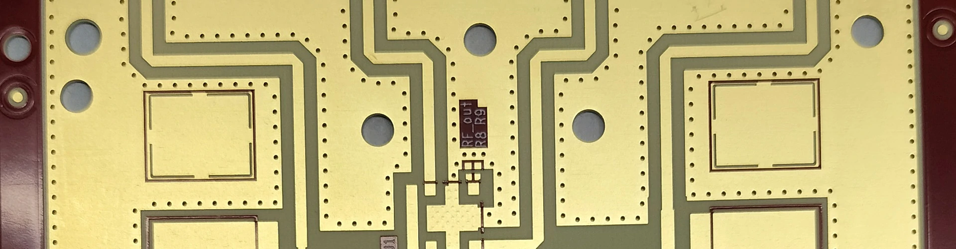
| RF launch and antenna areas | Surface access is often required |
| Short high-speed connections | Simple routing and easier debugging |
| Test points and probing | Easier oscilloscope or probe access |
| Low-to-medium layer count boards | Reduces internal routing complexity |
Microstrip can be very useful in high-speed PCB design, but it is more exposed to external noise, radiation, solder mask effects, and nearby copper structures. For this reason, it needs careful impedance control and enough spacing from other sensitive signals.
Stripline PCB Routing Explained
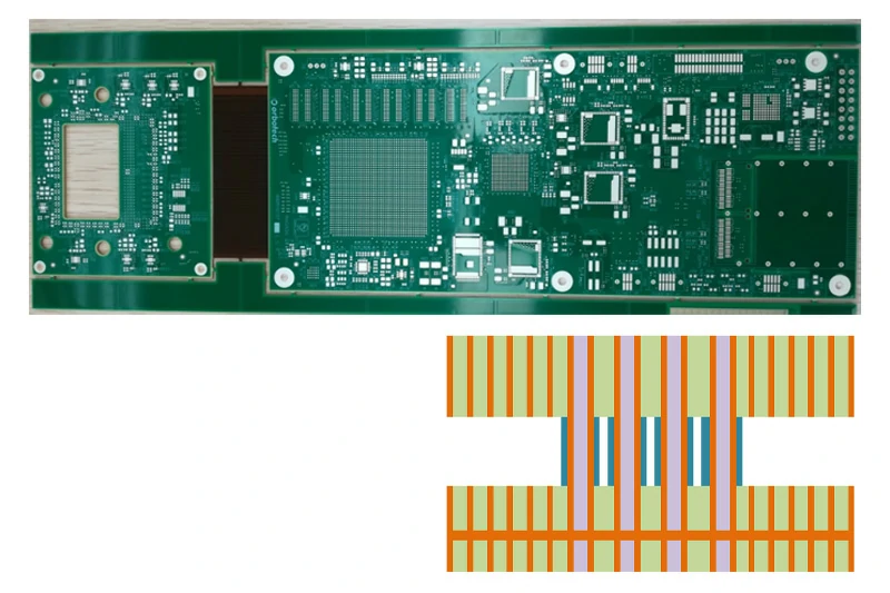
A stripline is routed inside the PCB, between two reference planes. Because it is embedded in dielectric material and surrounded by reference planes, stripline routing is more shielded than microstrip routing.
Stripline is commonly used for:
| Common Use Case | Why Stripline Is Used |
|---|---|
| Long high-speed routes | Better shielding and stable return paths |
| Dense multilayer boards | Efficient internal signal routing |
| EMI-sensitive designs | Lower external radiation risk |
| High-speed differential pairs | More controlled electromagnetic environment |
| Critical digital interfaces | Better isolation from external interference |
Stripline is often preferred for longer high-speed routes when EMI control, crosstalk reduction, and signal isolation are more important than surface access.
However, stripline also has trade-offs. It is harder to probe directly, requires multilayer PCB construction, may involve more via transitions, and is strongly dependent on dielectric thickness and material consistency.
Microstrip vs Stripline: Core Comparison Table
| Factor | Microstrip | Stripline |
|---|---|---|
| PCB layer position | Outer layer | Inner layer |
| Reference plane | Usually one adjacent plane | Two reference planes |
| EMI radiation | Higher risk | Lower risk |
| Crosstalk control | Moderate, depends on spacing and plane quality | Generally better due to shielding |
| Signal propagation | Often faster due to lower effective dielectric constant | Often slower because signal is fully in dielectric |
| Loss behavior | Can be lower in some applications | Can be higher depending on material and length |
| Probing and debugging | Easier | Harder |
| Fabrication complexity | Lower | Higher because it requires multilayer stackup |
| Environmental sensitivity | More affected by solder mask, air, nearby objects | More stable and enclosed |
| Best use | Short routes, RF access, breakout, testing | Long high-speed routes, EMI-sensitive signals, dense boards |
Which Routing Is Better for High-Speed PCB?
The practical answer is:
Use microstrip when you need surface access, shorter routing, easier testing, RF launch structures, or simpler fabrication. Use stripline when you need stronger shielding, lower radiation, better crosstalk control, or long internal high-speed routing.
In high-speed PCB design, “better” does not mean one routing type is always superior. It means the routing structure matches the electrical requirement and manufacturing capability.
For example:
- A short USB differential pair from a connector to a nearby IC may work well as microstrip.
- A long PCIe or SerDes route across a dense multilayer board may be better as stripline.
- An RF antenna feed may require microstrip or coplanar waveguide on the surface.
- A sensitive clock line inside an EMI-constrained product may benefit from stripline.
- A design that needs easy probing during validation may keep some signals as microstrip.
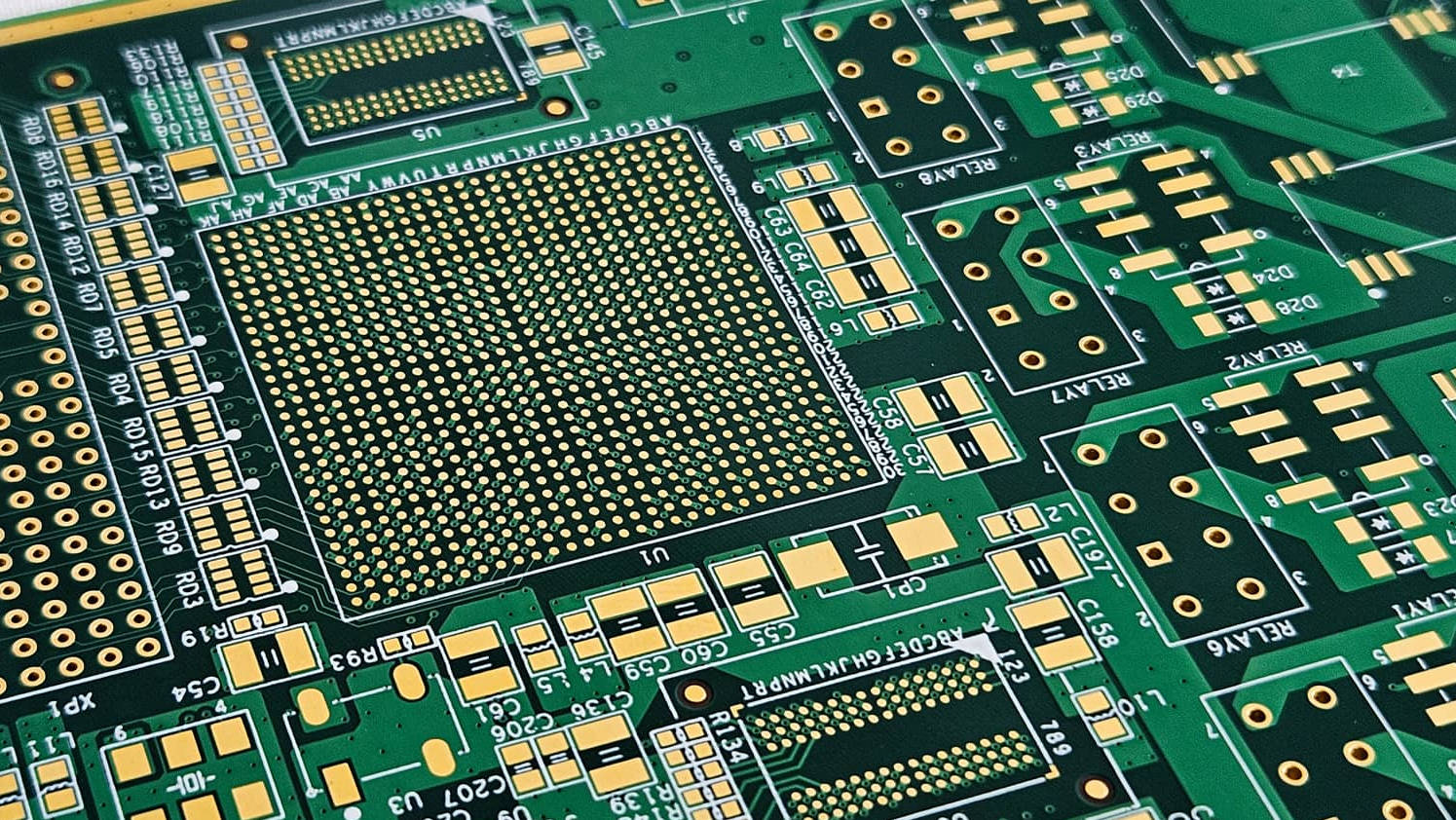
When the design involves multiple high-speed interfaces, a mixed strategy is common. Engineers may break out from BGA packages on microstrip layers, transition through vias, and then route longer sections as stripline.
Why This Choice Matters for B2B High-Speed PCB Projects
For companies sourcing high-speed PCBs, the microstrip vs stripline decision affects more than layout style. It influences manufacturing cost, impedance tolerance, stackup design, prototype success, signal integrity, EMI performance, and production repeatability.
A poor routing choice may lead to:
- Eye diagram degradation
- Signal reflection
- Excessive insertion loss
- Crosstalk between adjacent channels
- EMI compliance failure
- Unstable high-speed data transmission
- Repeated board revisions
- Longer product development cycles
High-speed PCB design depends heavily on stackup and routing. Altium notes that high-speed board design focuses on interconnect design, PCB stackup design, and routing, while ground planes near traces help maintain consistent impedance and clear return paths.
That means PCB manufacturing support should start before production. If your design uses controlled impedance microstrip or stripline routing, the manufacturer should review stackup, dielectric thickness, copper thickness, impedance tolerance, and material selection.
A qualified high-speed PCB fabrication service can help align the design intent with manufacturable stackup parameters.
Technical Principle: Why Microstrip and Stripline Behave Differently
The electrical behavior of microstrip and stripline is mainly determined by field distribution.
Microstrip Field Distribution
In microstrip routing, the signal trace is on the outer PCB layer. Its electromagnetic field spreads partly through the dielectric material and partly through the air or solder mask above the board.
This structure gives microstrip some advantages:
- Easier access for testing
- Simpler routing from surface components
- Often faster propagation than stripline
- Useful for RF structures and connector launches
But it also creates disadvantages:
- More radiation risk
- More sensitivity to surrounding copper
- More sensitivity to solder mask thickness
- Higher exposure to external interference
- More careful spacing required for crosstalk control
Stripline Field Distribution
In stripline routing, the signal trace is embedded between two reference planes. The field is mostly confined inside the dielectric region.
This structure gives stripline several advantages:
- Better shielding
- Lower radiation risk
- More stable return path
- Better isolation from external objects
- Often better for dense high-speed internal routing
Its disadvantages include:
- More difficult probing
- More complex stackup requirements
- Stronger dependence on dielectric material
- Potentially greater loss over long distances
- More via transitions may be needed from surface components
Controlled Impedance: The Key Link Between Routing and Manufacturing
Microstrip and stripline are both commonly used as controlled impedance transmission lines. Controlled impedance means managing the characteristic impedance of a PCB transmission line formed by traces and reference planes. It is affected by physical dimensions and dielectric materials. Cadence lists common controlled impedance structures including single-ended microstrip, single-ended stripline, differential microstrip, and differential stripline.
For manufacturing, impedance is affected by:
| Parameter | Effect on Routing Performance |
|---|---|
| Trace width | Influences single-ended and differential impedance |
| Trace spacing | Critical for differential pairs and crosstalk |
| Copper thickness | Affects impedance and etching tolerance |
| Dielectric thickness | Affects impedance and field confinement |
| Dielectric constant | Affects propagation delay and impedance |
| Solder mask | More relevant to microstrip than stripline |
| Reference plane distance | Determines field distribution and return path |
| Fabrication tolerance | Affects production consistency |
A microstrip or stripline design should not be judged only by its routing geometry; it must be evaluated as part of the full PCB stackup and fabrication process.
When sending a high-speed PCB project for quotation, provide impedance targets, stackup requirements, material preference, layer assignment, and critical net information. This allows the PCB manufacturer to check whether the routing structure can be produced within realistic process tolerances.
Microstrip Advantages and Limitations
Advantages of Microstrip
Microstrip is widely used because it is practical, accessible, and suitable for many high-speed layouts.
Main advantages include:
- Easier routing from surface-mounted components
- Easier probing and debugging
- Lower fabrication complexity
- Useful for RF launch areas and antennas
- Suitable for short high-speed connections
- Less dependent on inner-layer lamination accuracy
Microstrip can be a good choice when the route is short, the EMI requirement is manageable, and surface access is needed.
Limitations of Microstrip
Microstrip is more exposed than stripline. This makes it more vulnerable to radiation, external coupling, and environmental variation.
Common limitations include:
- Higher EMI radiation risk
- More sensitivity to solder mask thickness
- More coupling to nearby traces or copper pours
- Less shielding than stripline
- More careful spacing required in dense routing areas
For this reason, microstrip may not be ideal for long, high-speed, EMI-sensitive routes unless carefully designed and verified.
Stripline Advantages and Limitations
Advantages of Stripline
Stripline provides a more enclosed transmission environment. This makes it attractive for high-speed signals that need better isolation.
Main advantages include:
- Better EMI control
- Lower radiation risk
- Better shielding from external interference
- More stable reference environment
- Suitable for long internal high-speed routing
- Useful for dense multilayer boards
Stripline is often preferred when a design must meet strict signal integrity and EMI requirements.
Limitations of Stripline
Stripline is not always the simplest choice. It requires a multilayer PCB and more careful stackup planning.
Common limitations include:
- Harder to probe and debug
- Higher manufacturing complexity
- More dependent on dielectric thickness control
- May require more vias from surface components
- Can increase cost if additional layers are needed
If a project is cost-sensitive and the high-speed routes are short, microstrip may be more practical.
Microstrip vs Stripline for Differential Pairs
Differential pairs are widely used in high-speed PCB design. They can be routed as edge-coupled microstrip, edge-coupled stripline, or other variations depending on stackup and design requirements.
| Differential Pair Factor | Microstrip Differential Pair | Stripline Differential Pair |
|---|---|---|
| Accessibility | Easier to probe | Harder to probe |
| EMI control | Moderate | Better |
| Routing density | Limited on outer layers | Better for internal routing |
| Impedance stability | Affected by solder mask and surface conditions | More stable if dielectric is controlled |
| Common applications | USB, short connector routes, RF-related breakout | PCIe, SerDes, Ethernet, longer high-speed channels |
| Manufacturing concern | Solder mask and surface copper effects | Lamination and dielectric thickness control |
For BGA breakout, engineers may start with microstrip, then transition to stripline for longer route sections. The key is to maintain impedance continuity, minimize via discontinuities, and preserve a clean return path.
Engineering Decision Matrix: When to Use Each Routing Type
| Design Situation | Better Routing Choice | Reason |
|---|---|---|
| Short route from connector to IC | Microstrip | Easy access and simple routing |
| Long high-speed route across board | Stripline | Better shielding and lower radiation |
| RF antenna feed | Microstrip or coplanar structure | Surface electromagnetic behavior may be required |
| EMI-sensitive enclosure | Stripline | Reduced radiation risk |
| Prototype requiring frequent probing | Microstrip | Easier validation |
| Dense multilayer digital board | Stripline | Better internal routing control |
| Low-cost, moderate-speed board | Microstrip | Lower complexity |
| Critical SerDes channel | Often stripline, depending on stackup | Better isolation and controlled path |
| BGA breakout area | Mixed | Microstrip breakout, stripline escape routing |
| Strict impedance and length matching | Either, if stackup is controlled | Depends on interface and routing plan |
Common Mistakes in Microstrip and Stripline Routing
Mistake 1: Choosing Routing Type After Layout Is Almost Finished
Microstrip and stripline decisions should be made during stackup planning. If the layer structure is not suitable, layout adjustments may not solve the problem later.
Mistake 2: Ignoring Return Path Continuity
Both microstrip and stripline need a clean reference path. Routing over splits, voids, or poorly connected planes can create impedance discontinuity and EMI problems.
Mistake 3: Assuming Stripline Automatically Solves All Problems
Stripline reduces radiation risk, but it still requires proper impedance control, spacing, via design, and material selection.
Mistake 4: Using Microstrip for Long Noisy Routes Without Review
Microstrip can work well, but long exposed traces can increase radiation and coupling risk, especially in dense boards.
Mistake 5: Sending Only Gerber Files Without Stackup Requirements
For high-speed PCB manufacturing, Gerber files alone may not communicate impedance intent. The supplier needs stackup, impedance values, controlled layers, and critical net information.
Manufacturing Considerations for Microstrip and Stripline PCBs
From a manufacturing perspective, both routing structures require accurate process control. However, the risk points are different.
| Manufacturing Factor | Microstrip Concern | Stripline Concern |
|---|---|---|
| Copper etching | Trace width affects impedance | Trace width affects impedance |
| Dielectric thickness | Distance to reference plane matters | Distance between planes matters |
| Solder mask | Can affect outer-layer impedance | Usually less direct effect |
| Lamination | Less complex | More critical |
| Impedance testing | Common for controlled traces | Common for controlled traces |
| Material consistency | Important | Very important |
| Layer registration | Important | Important for multilayer alignment |
| Via design | Needed for transitions | Often more important due to internal routing |
For production, your supplier should confirm whether impedance coupons, TDR testing, or stackup adjustment are needed. Cadence notes that impedance control involves dielectric thickness, trace width, and spacing, and that manufacturers may use TDR coupons to verify impedance targets.
This is why early communication with a controlled impedance PCB manufacturer is important for high-speed boards.
How to Choose a PCB Supplier for Microstrip and Stripline High-Speed Boards
A high-speed PCB supplier should not only manufacture copper patterns. The supplier should understand the relationship between routing structure, impedance, stackup, material selection, and fabrication tolerance.
When evaluating a supplier, check whether they can support:
- Controlled impedance microstrip and stripline structures
- Single-ended and differential impedance requirements
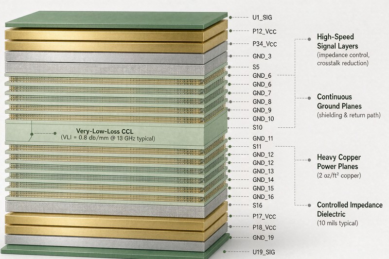
- Multilayer stackup review
- Material selection for high-speed applications
- Dielectric thickness and copper thickness control
- Impedance coupon testing when required
- Engineering communication before production
- Prototype and volume production consistency
For purchasing teams, the key question is not only “Can you make this board?” A better question is: “Can you manufacture this high-speed PCB according to the impedance, stackup, and signal integrity requirements?”
If your design includes microstrip and stripline routing, choose a high-speed PCB supplier that can review the stackup before fabrication and communicate manufacturability risks clearly.
Practical Checklist Before Fabrication
Before submitting your high-speed PCB files, prepare the following information:
| Item | Why It Matters |
|---|---|
| Layer stackup | Defines microstrip and stripline structures |
| Controlled impedance table | Tells the manufacturer target impedance values |
| Critical net list | Helps identify high-speed routes |
| Material requirement | Affects dielectric constant and signal loss |
| Copper thickness | Affects impedance and manufacturability |
| Differential pair rules | Supports correct spacing and length matching |
| Via structure | Affects transition quality |
| Surface finish | Important for assembly and long-term reliability |
| Test requirement | Clarifies impedance verification expectations |
This checklist can reduce misunderstandings between the design team and PCB manufacturer, especially when the board includes both surface microstrip and internal stripline routing.
FAQ
1. Is microstrip or stripline better for high-speed PCB routing?
Microstrip is better for short surface routes, RF access, and easier probing. Stripline is better for longer internal high-speed routes, EMI control, and reduced radiation. The better choice depends on stackup, signal speed, impedance target, and product requirements.
2. What is the main difference between microstrip and stripline PCB routing?
The main difference is location in the PCB stackup. Microstrip is usually routed on an outer layer with one reference plane, while stripline is routed inside the board between two reference planes.
3. Does stripline have less EMI than microstrip?
In many high-speed PCB applications, stripline has lower radiation risk because it is embedded between reference planes. However, EMI performance also depends on return path quality, via transitions, spacing, grounding, and overall board design.
4. Is microstrip easier to manufacture than stripline?
Microstrip is generally easier to route, inspect, and probe because it is on the outer layer. Stripline requires multilayer stackup control and is harder to access after fabrication, but it is commonly used in advanced high-speed PCB designs.
5. Which is better for differential pair routing, microstrip or stripline?
Both can be used for differential pairs. Microstrip is often useful for short connector or breakout routes, while stripline is often preferred for longer high-speed differential pairs that need better shielding and EMI control.
6. Does controlled impedance apply to both microstrip and stripline?
Yes. Both microstrip and stripline can be designed as controlled impedance transmission lines. The final impedance depends on trace width, spacing, copper thickness, dielectric thickness, dielectric constant, and reference plane structure.
7. When should I discuss microstrip and stripline routing with my PCB manufacturer?
You should discuss it before final layout or before fabrication quotation. Early stackup review helps confirm whether the target impedance, materials, dielectric thickness, and layer structure are manufacturable.
Conclusion
Microstrip and stripline are both important routing structures in high-speed PCB design. Microstrip is practical for surface routing, component breakout, RF access, short high-speed routes, and easier debugging. Stripline is more suitable for internal high-speed routing, EMI-sensitive signals, long differential pairs, and dense multilayer boards that require better shielding.
The right choice is not microstrip or stripline alone, but the routing structure that matches your stackup, impedance target, signal integrity requirement, and manufacturing capability.
For B2B projects, this decision should be made before production with clear communication between the design team and PCB manufacturer. If your project involves controlled impedance, differential pairs, dense multilayer routing, or strict signal integrity requirements, working with an experienced high-speed PCB manufacturer can help reduce design-to-production risk.