The core difference between a Multilayer PCB and an HDI (High-Density Interconnect) PCB lies in their density and manufacturing technology. While all HDI PCBs are multilayer boards, not all multilayer PCBs are HDI. The distinction comes from HDI PCBs utilizing advanced technologies like microvias, thinner traces, and smaller component pads to pack significantly more functionality into a smaller, lighter, and higher-performing circuit board. Standard multilayer PCBs use traditional mechanically drilled vias and have lower component and routing density in comparison.
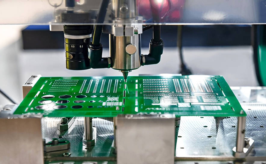
Table of Contents
- 1. What is a Multilayer PCB? A Foundational Technology
- 2. What is an HDI PCB? The Evolution of Density
- 3. Key Differences: Multilayer vs. HDI PCB Head-to-Head
- 4. Comparison Table: Multilayer PCB vs. HDI PCB at a Glance
- 5. When Should You Choose an HDI PCB Over a Standard Multilayer PCB?
- 6. Conclusion: Choosing the Right Board for Your Project
What is a Multilayer PCB? A Foundational Technology
A multilayer printed circuit board (PCB) is a circuit board comprised of more than two conductive copper layers. These boards are essentially a stack of double-sided PCBs laminated and bonded together with layers of insulation (prepreg) in between. The primary purpose of adding layers is to provide more surface area for wiring and to accommodate complex circuits that cannot be routed on a single or double-sided board. This structure allows for greater circuit density and simplified designs for intricate electronic devices.
Construction and Characteristics
The construction of a standard multilayer PCB relies on conventional fabrication techniques. The layers are interconnected using various types of vias, which are holes drilled through the board and plated with copper to create an electrical path.
- Through-Hole Vias: These are the most common type, drilled from the top layer to the bottom layer, passing through all internal layers, whether they connect to them or not. They are simple and cheap to produce but take up valuable board space on every layer.
- Blind Vias: These connect an external layer to one or more internal layers but do not pass through the entire board. They are more space-efficient than through-holes but add to the manufacturing complexity and cost.
- Buried Vias: These connect two or more internal layers without reaching either external layer. They are excellent for increasing routing density but are the most complex and expensive type of via in standard multilayer fabrication.
The trace and space widths on these boards are typically larger, and the drilling process is mechanical, which limits how small and close together the features can be.
Advantages and Limitations of Multilayer PCBs
Multilayer PCBs have long been the workhorse of the electronics industry due to their balance of capability and cost. Their primary advantage is the ability to support highly complex circuitry in a single, robust component. They offer good EMI (electromagnetic interference) shielding by incorporating ground and power planes. However, they have limitations, especially as electronics continue to shrink. The use of larger, mechanically drilled vias and wider traces means they can only achieve a certain level of density. As component sizes shrink and pin counts increase, standard multilayer boards can become large, heavy, and electrically constrained.
What is an HDI PCB? The Evolution of Density
High-Density Interconnect (HDI) technology is a direct response to the demand for smaller, faster, and more powerful electronics. An HDI PCB is an advanced type of multilayer PCB that features significantly higher wiring and component density per unit area. This is achieved by moving beyond traditional manufacturing methods and embracing more sophisticated techniques that allow for finer lines, tighter spacing, and, most importantly, a different class of interconnects known as microvias.
The Role of Microvias and Advanced Features
The defining feature of an HDI PCB is the microvia. Unlike a traditional mechanically drilled via, a microvia is typically laser-drilled and has a diameter of 150 microns (0.15mm) or less. This incredibly small size is the key to unlocking higher density.
- Laser-Drilled Microvias: These small vias free up immense amounts of board real estate. Because they only span one layer (or a pair of layers), they create more available routing space on inner layers, a concept known as “via-in-pad” technology.
- Via-in-Pad (VIP): This process allows vias to be placed directly on the copper pads of surface-mount components. This shortens the electrical path, improving signal integrity, and dramatically increases the density around complex components like BGAs (Ball Grid Arrays).
- Finer Traces and Spaces: HDI manufacturing processes enable conductor traces and the spaces between them to be much narrower, often below 100 microns, allowing more connections in a smaller area.
- Sequential Lamination: HDI boards are built layer by layer using a process called sequential lamination. This allows for the creation of complex structures with stacked and staggered microvias, further optimizing space.
Why Choose an HDI PCB? Key Benefits
The move to HDI technology brings substantial benefits, particularly for high-performance applications. The primary advantage is miniaturization—the ability to create smaller and lighter products without sacrificing functionality. For example, the complex boards inside smartphones, tablets, and wearables are all HDI PCBs. Furthermore, the shorter connection paths and smaller via stubs in HDI designs lead to superior electrical performance, including better signal integrity, reduced signal reflection, and lower EMI. While the initial manufacturing cost can be higher, HDI can sometimes be more cost-effective overall by reducing a design from, say, an 8-layer standard board to a 6-layer HDI board, saving material and lamination costs.
Key Differences: Multilayer vs. HDI PCB Head-to-Head
Understanding the fundamental distinctions between these two technologies is crucial for making the right design and manufacturing choices. The differences span from the physical vias to electrical performance and cost.
Via Technology: Mechanical Drilling vs. Laser Ablation
This is the most significant differentiator. Standard multilayer PCBs rely on mechanical drills to create vias, which have a larger aspect ratio (depth-to-diameter) and size. This process is less precise and requires larger annular rings (the copper pad around the via), consuming valuable board space. In contrast, HDI PCBs use high-precision laser ablation to create microvias. Laser drilling is faster, more accurate, and creates much smaller holes, enabling technologies like via-in-pad that are impossible with mechanical drills.
Circuit Density, Size, and Weight
The direct result of microvia technology is a dramatic increase in density. HDI PCBs can accommodate more components and more routing in the same or smaller area. This allows engineers to design products that are significantly smaller and lighter than their multilayer counterparts. A device that might require a 10-layer standard multilayer board could potentially be designed on a 6 or 8-layer HDI board, reducing both the final thickness and weight of the product.
Performance and Signal Integrity
In high-frequency applications, electrical performance is paramount. HDI PCBs offer a distinct advantage. The smaller vias and shorter trace lengths reduce parasitic capacitance and inductance, which are detrimental to signal integrity. This leads to cleaner signals, less noise, and reduced cross-talk between traces. The ability to use via-in-pad also shortens the path from a component to a via, minimizing signal reflections and improving performance for high-speed digital and RF circuits.
Cost Implications and Overall Value
On a per-board basis, an HDI PCB is generally more expensive to manufacture due to the advanced laser drilling, sequential lamination, and tighter tolerances required. However, considering the total system cost can change the perspective. By reducing the layer count and board size, HDI can lead to material savings. More importantly, the improved performance and smaller form factor can provide a competitive advantage that outweighs the initial fabrication cost, making it a better value proposition for cutting-edge products.
Comparison Table: Multilayer PCB vs. HDI PCB at a Glance
This table provides a clear, side-by-side summary of the main characteristics of standard multilayer and HDI PCBs.
| Feature | Standard Multilayer PCB | HDI PCB |
|---|---|---|
| Via Technology | Mechanical drilling (Through-hole, Blind, Buried) | Laser ablation (Microvias, stacked/staggered vias) |
| Typical Via Size | > 150 microns | ≤ 150 microns |
| Component Density | Standard to Moderate | High to Very High |
| Trace/Space Width | Typically ≥ 4-5 mils (100-125 microns) | Typically ≤ 3-4 mils (75-100 microns) |
| Layer Count | Can be high, but often requires more layers for the same complexity | Can achieve same complexity with fewer layers |
| Electrical Performance | Good, but can be limited by via stubs and longer trace lengths | Excellent, with superior signal integrity and reduced EMI |
| Cost | Lower initial fabrication cost | Higher initial fabrication cost, but potential for lower system cost |
| Common Applications | Servers, desktop computers, industrial controls, larger consumer electronics | Smartphones, tablets, wearables, medical devices, aerospace electronics |
When Should You Choose an HDI PCB Over a Standard Multilayer PCB?
The decision to use an HDI board is driven by specific project requirements. While a standard multilayer PCB is sufficient for many applications, you should strongly consider transitioning to HDI technology in the following scenarios:
- Miniaturization is Critical: If your product’s primary selling point is its small size and light weight (e.g., wearables, drones, portable medical sensors), HDI is not just an option—it’s a necessity.
- High-Pin-Count Components: When using fine-pitch BGAs or other components with a high number of I/O pins, HDI’s via-in-pad capability is often the only way to successfully route all the connections without dramatically increasing the board size or layer count.
- High-Frequency Performance is Required: For applications involving high-speed data transfer, RF communication, or sensitive analog signals, the superior signal integrity of HDI boards is a major advantage. The shorter signal paths minimize distortion and signal loss.
- You Need to Reduce Layer Count: If a standard multilayer design is resulting in a high layer count (e.g., 12+ layers) and becoming thick, complex, and expensive, an HDI redesign could potentially achieve the same routing with fewer layers, simplifying the stackup and possibly reducing overall cost.
Conclusion: Choosing the Right Board for Your Project
In summary, the choice between a multilayer PCB and an HDI PCB is a trade-off between density, performance, and cost. A standard multilayer PCB is a reliable and cost-effective solution for a wide range of electronics where space and extreme performance are not the primary constraints. However, as technology pushes towards ever-smaller and more powerful devices, the HDI PCB has become the clear successor. It represents an evolution in manufacturing, enabling the creation of compact, lightweight, and high-performing products that were previously impossible. By understanding the core differences—centered around via technology and density—engineers and designers can make an informed decision that aligns with both their technical requirements and business goals.
Multilayer PCB vs HDI PCB, what is the difference between multilayer and HDI PCB, high density interconnect PCB, HDI PCB advantages, microvia technology, laser drilled vias, when to use HDI PCB, multilayer PCB limitations, HDI PCB cost, circuit board technology

