PCB Wire Bonding: The Ultimate Guide to Modern Interconnection Technology
Key Comparison: PCB Wire Bonding vs. Alternative Technologies
Feature | Wire Bonding | Flip-Chip Bonding | Wafer-Level Packaging |
Initial Cost | Lower investment | Higher investment | Highest investment |
Reliability | Proven (80%+ market share) | High reliability | Very high reliability |
Production Speed | Moderate | Fast | Fastest |
Miniaturization | Limited by wire diameter | Better for high density | Best for ultra-high density |
Best Applications | Automotive, industrial electronics | Advanced consumer electronics | Cutting-edge telecom & computing |
Market Size (2024) | $4.52 Billion | Part of $8.7B flip chip market | Part of $3.8B WLP market |
What is PCB Wire Bonding?
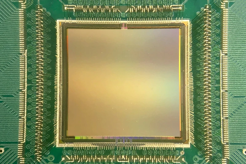
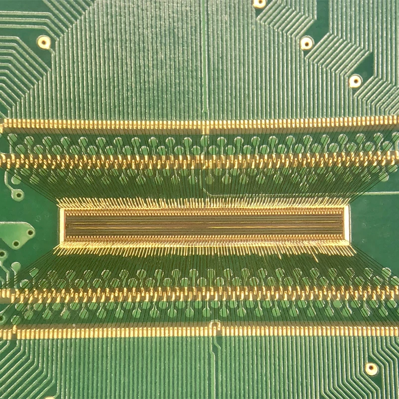
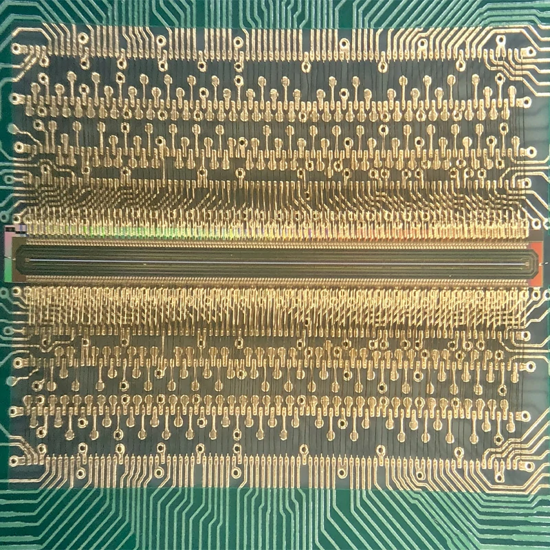
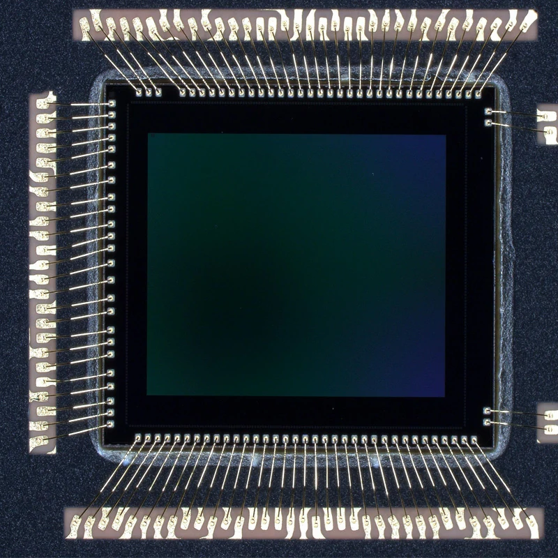
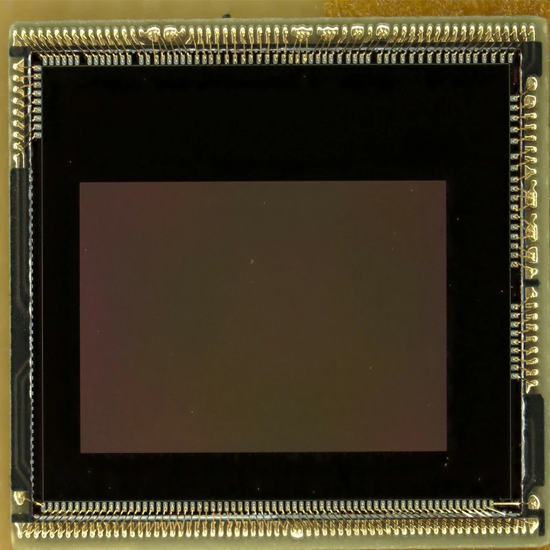
PCB wire bonding is a critical interconnection technology that creates electrical pathways between semiconductor chips and external circuits. In simple terms, it uses extremely thin wires to connect the tiny bond pads on an integrated circuit (IC) chip to the contact points on a printed circuit board (PCB) or package substrate.
The Critical Role of Wire Bonding in Electronics
Wire bonding serves as the vital link that allows complex electronic systems to function properly. Without these microscopic connections, the powerful processors in your smartphone or the safety systems in your car would be useless silicon chips with no way to communicate with the outside world.
Key Components of a Wire Bond
A typical wire bond consists of:
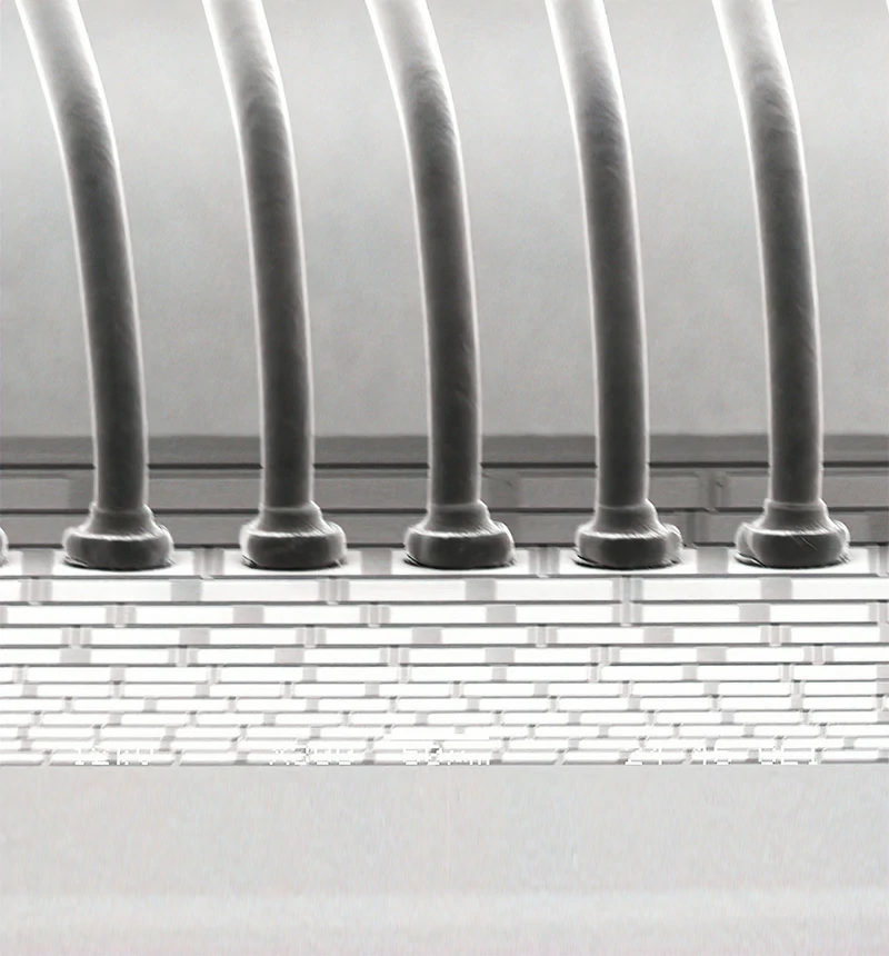
- Bond wire - Usually gold, aluminum, or copper with diameters between 15-33 micrometers (thinner than a human hair)
- First bond - Connection to the semiconductor die
- Wire loop - Carefully shaped path between connections
- Second bond - Connection to the substrate or leadframe
- Encapsulation - Protective covering that preserves the integrity of the bond
Types of Wire Bonding Techniques in PCB Manufacturing
Different applications require specific wire bonding approaches. Let’s explore the major techniques used in modern PCB manufacturing
Advantages of Wedge Bonding
- Lower loop height - Ideal for thin packages
- Works well with aluminum - Perfect for cost-sensitive applications
- Lower heat requirements - Suitable for temperature-sensitive components
- Precise placement - Offers excellent accuracy for critical connections
Limitations of Wedge Bonding
- Slower process - Typically 4-8 bonds per second
- Directional constraints - Second bond must align with first bond
- Less common equipment - Fewer vendors offer specialized wedge bonders
Thermocompression Bonding:
Heat-Driven Performance
Thermocompression bonding relies primarily on heat and pressure, with little or no ultrasonic energy. This technique creates bonds through atomic diffusion at the interface between the wire and bond pad.
Applications of Thermocompression Bonding
- High-temperature electronics
- Gold-to-gold connections
- Wafer-level bonding processes
- Military and space applications requiring extreme reliability
Thermosonic Bonding:
The Best of Both Worlds
Thermosonic bonding combines ultrasonic energy with heat and pressure. This hybrid approach offers excellent versatility and is widely used for high-reliability applications.
Key Features of Thermosonic Bonding
- Uses moderate heat (100-150°C) with ultrasonic assistance
- Creates strong intermetallic bonds
- Works excellently with gold and copper wires
- Widely used in automotive and aerospace applications
Ultrasonic Bonding:
Cold Welding Approach
Pure ultrasonic bonding uses mechanical vibration without significant heat. This “cold welding” process is ideal for temperature-sensitive components and aluminum wire applications.
Benefits of Ultrasonic Bonding
- Minimal thermal stress on components
- Energy efficient process
- Lower risk of thermal damage
- Excellent for aluminum wire bonding
- Reduced intermetallic formation
The Wire Bonding Process: Step-by-Step
Understanding the wire bonding process helps engineers optimize their designs for manufacturability and reliability. Let’s break down each stage of this precision manufacturing process
Pre-Bonding Preparation
Before actual bonding begins, several critical preparation steps ensure successful outcomes:
Die Attachment and Substrate Preparation
The semiconductor die must be securely attached to the substrate using either:
- Die attach adhesive - Epoxy-based materials for standard applications
- Eutectic bonding - Metal alloy bonding for high-reliability needs
- Solder attachment - For power applications requiring excellent thermal performance
The substrate must be thoroughly cleaned to remove contaminants that could compromise bond integrity.
Surface Cleaning and Activation
Bond pads on both the die and substrate undergo:
- Plasma cleaning to remove organic contaminants
- Chemical treatments to remove oxides
- Surface activation to promote strong metallic bonds
Equipment Setup and Calibration
Modern wire bonders require precise calibration of:
- Bond force parameters
- Ultrasonic energy levels
- Temperature settings
- Wire feed mechanisms
- Vision systems for alignment
The Main Bonding Sequence
The actual bonding process consists of several precisely controlled steps:
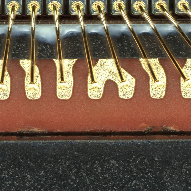
First Bond Formation (Die Side)
- The wire is fed through the bonding tool (capillary)
- For ball bonding, an electronic flame-off creates a ball at the wire tip
- The capillary positions precisely over the bond pad
- The tool applies pressure, heat, and/or ultrasonic energy
- A metallurgical bond forms between the wire and pad
The substrate must be thoroughly cleaned to remove contaminants that could compromise bond integrity.
Wire Loop Formation
After the first bond, the wire must form a carefully controlled loop:
- Loop height must balance clearance and package thickness requirements
- Loop profile affects reliability under thermal cycling and vibration
- Surface activation to promote strong metallic bonds
Second Bond Formation (Substrate Side)
- The capillary moves to the second bond location
- Pressure and energy are applied to create the second bond
- For ball bonding, this forms a "stitch" or "wedge" bond
- Wire feed mechanisms
- For wedge bonding, this creates another wedge-shaped bond
Wire Termination and Tail Formation
After the second bond:
- The wire is clamped
- The capillary moves up slightly
- A tail of appropriate length is formed for the next ball
- The wire is severed using mechanical force or an electronic flame-off
The substrate must be thoroughly cleaned to remove contaminants that could compromise bond integrity.
Post-Bonding Operations
Several important steps follow the basic bonding process:
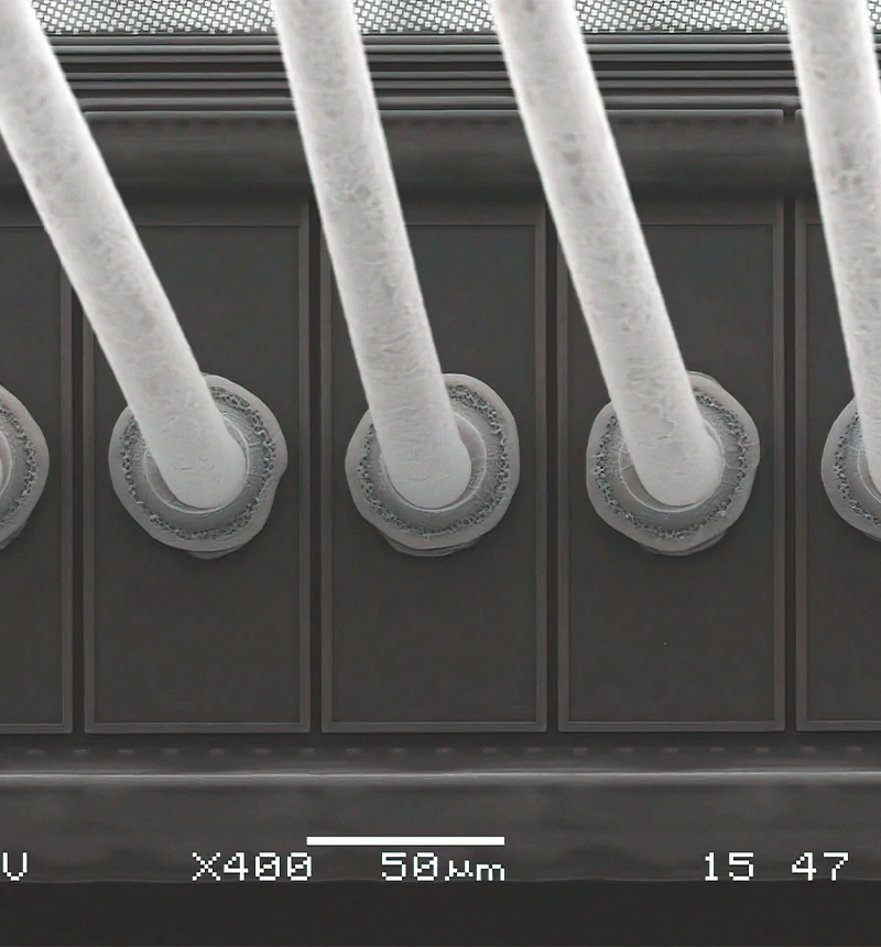
Visual Inspection
Automated optical inspection systems examine:
- Bond placement accuracy
- Bond size and shape
- Loop height and profile
- Signs of contamination or damage
Pull and Shear Testing
Destructive testing on sample bonds confirms strength:
- Pull tests measure the force required to break the wire
- Shear tests measure the force required to dislodge the bond
- Results must meet industry standards like MIL-STD-883
Non-Destructive Testing
Advanced inspection techniques include:
- Ultrasonic imaging to detect internal voids
- X-ray inspection for hidden defects
- Electrical testing for continuity and resistance
Encapsulation and Protection
Finally, wire bonds are protected with:
- Molding compounds for standard packages
- Specialized coatings for harsh environments
- Hermetic sealing for military and space applications
Materials and Wire Diameter Selection for PCB Wire Bonding
The choice of bonding wire material and diameter significantly impacts performance, reliability, and cost. Let’s examine the key considerations when selecting these critical components.
Gold Wire: The Traditional Premium Choice
Gold (Au) has historically been the preferred wire bonding material due to its outstanding properties.
Advantages of Gold Wire
- Superior conductivity - Ensures minimal electrical resistance
- Excellent corrosion resistance - Maintains performance over time
- High reliability - Proven track record in critical applications
- Workability - Easy to form consistent balls for ball bonding
- Compatibility - Works well with a variety of pad materials
Challenges with Gold Wire
- Cost - Gold's high price significantly impacts production expenses
- Heavy weight - Can create stress on delicate components
- Market volatility - Price fluctuations complicate budgeting
Aluminum Wire: Cost-Effective Alternative
Aluminum (Al) offers a more economical option that works well for many applications.
Advantages of Aluminum Wire
- Cost savings - Significantly less expensive than gold
- Lightweight - Reduces stress on connections
- Natural oxide layer - Provides some environmental protection
- Excellent for wedge bonding - Industry standard for this technique
Challenges with Aluminum Wire
- Susceptibility to corrosion - Requires careful environmental control
- Lower electrical conductivity - May impact high-performance applications
- Potential for intermetallic growth - Can create reliability issues with certain pad materials
- Less suitable for ball bonding - Mainly used in wedge bonding applications
Copper Wire: The Modern Standard
Copper (Cu) has emerged as the preferred material for many modern applications, offering an excellent balance of performance and cost.
Advantages of Copper Wire
- Cost efficiency - Approximately 1/10 the cost of gold
- Superior electrical conductivity - Better than gold in some metrics
- Excellent thermal conductivity - Helps dissipate heat from dies
- Higher stiffness - Can maintain loop shapes more reliably
- Better intermetallic formation - Potentially more stable long-term bonds
Challenges with Copper Wire
- Oxidation tendency - Requires controlled atmospheres during bonding
- Higher hardness - Can damage delicate pads without precise force control
- Specialized equipment - May require upgraded or specialized bonding machines
- Narrower process window - Less forgiving of parameter variations
Specialized Wire Options
Several specialized wire options address specific application needs:
Palladium-Coated Copper (PCC)
- Combines copper's conductivity with improved oxidation resistance
- Increasingly popular for fine-pitch applications
- Offers a middle ground between copper and gold in terms of cost and performance
Silver Wire
- Growing in popularity for certain applications
- Better conductivity than copper
- Less expensive than gold
- Requires careful environmental controls to prevent tarnishing
Coated and Alloyed Wires
- Gold-plated copper combines benefits of both materials
- Copper-silver alloys offer enhanced reliability
- Specialized coatings can improve bonding characteristics
Wire Diameter Selection Factors
Selecting the appropriate wire diameter involves balancing several considerations:
Technical Requirements
- Current carrying capacity - Higher currents require larger diameters
- Bond pad size - Smaller pads necessitate thinner wires
- Pitch limitations - Fine-pitch applications demand thinner wires
- Loop height restrictions - Package thickness may limit wire size
Common Wire Diameters
- 18-25 µm - Standard for most consumer electronics
- 15-18 µm - Fine-pitch applications like smartphones
- 25-33 µm - Power applications requiring higher current capacity
- >33 µm - Specialized power modules and automotive applications
Impact of Diameter on Process and Performance
- Thinner wires require more precise bonding parameters
- Thicker wires offer better current handling but limit miniaturization
- Wire diameter affects loop stability during molding processes
- Different diameters may require different bonding tools (capillaries)
Real-World Applications of PCB Wire Bonding
Wire bonding technology plays a crucial role across numerous industries. Let’s explore how this versatile interconnection method is applied in various sectors.
Semiconductor Packaging Applications
The semiconductor industry relies heavily on wire bonding for connecting dies to packages.
Integrated Circuit Packages
- QFP (Quad Flat Package) - Uses wire bonds to connect die to leads on four sides
- BGA (Ball Grid Array) - Often combines wire bonding with substrate connections
- SIP (System in Package) - Uses wire bonds to connect multiple dies within a single package
- QFN (Quad Flat No-leads) - Utilizes wire bonding for internal connections
Memory Device Manufacturing
- DRAM modules frequently use wire bonding for die-to-substrate connections
- Flash memory devices employ wire bonding for reliable connections
- High-bandwidth memory increasingly uses advanced wire bonding techniques
Microprocessor Assembly
- Wire bonding connects processor cores to package substrates
- Power delivery circuits utilize heavier gauge wire bonds
- I/O interfaces rely on fine-pitch wire bonding for high-density connections
Automotive Electronics Applications
The automotive industry has unique requirements that make wire bonding particularly valuable.
Powertrain Control Modules
- Engine controllers use wire bonding for reliable connections
- Transmission control units rely on robust wire bonding
- Hybrid and electric vehicle power modules use heavy gauge wire bonds
Safety Systems
- Airbag controllers employ wire bonding for mission-critical reliability
- Anti-lock brake systems utilize wire bonds in control modules
- Advanced driver assistance systems (ADAS) rely on wire bonding for sensor integration
Automotive-grade wire bonding with heavy copper wire for high current applications
Infotainment and Connectivity
- Head units utilize wire bonding for processor connections
- Connectivity modules employ fine-pitch bonding for RF components
- Display controllers rely on high-density wire bonding
Consumer Electronics Implementation
Consumer devices represent the highest volume application for wire bonding technology.
Smartphone Components
- Application processors use thousands of wire bonds per device
- Camera modules employ wire bonding for sensor connections
- Power management ICs utilize wire bonding for reliable power delivery
Wearable Technology
- Smartwatches use fine-pitch wire bonding to save space
- Fitness trackers employ wire bonding for sensor connections
- Hearable devices utilize miniaturized wire bonding techniques
Home Entertainment Systems
- Smart TV processors rely on wire bonding for connections
- Audio amplifiers use wire bonding for power and signal routing
- Gaming consoles employ wire bonding for GPU and CPU packages
Industrial and Medical Electronics
Specialized applications require the highest reliability levels for wire bonding.
Industrial Control Systems
- Programmable logic controllers (PLCs) use wire bonding for processor connections
- Motor drives employ heavy gauge wire bonding for power handling
- Sensor interfaces rely on wire bonding for signal integrity
Medical Implantable Devices
- Pacemakers utilize ultra-reliable gold wire bonding
- Cochlear implants employ fine-pitch wire bonding for miniaturization
- Neuromodulation devices use specialized wire bonding techniques
Test and Measurement Equipment
- Oscilloscopes rely on wire bonding for analog front-end ICs
- Spectrum analyzers employ wire bonding for RF component connections
- Industrial sensors utilize wire bonding for reliability in harsh environments
Advantages and Limitations of Wire Bonding Technology
Wire bonding offers distinct benefits but also comes with certain constraints. Understanding these factors helps engineers make informed decisions for their specific applications.
Key Advantages of Wire Bonding
Wire bonding remains the dominant interconnection technology in electronics for several compelling reasons.
Proven Reliability and Maturity
- Extensive track record - Over 60 years of continuous refinement
- Well-documented performance - Comprehensive industry standards and testing procedures
- High yield rates - Typically exceeds 99.9% in production environments
- Predictable failure modes - Well-understood reliability models
Cost-Effectiveness for Many Applications
- Lower initial equipment investment compared to flip-chip or wafer-level packaging
- Flexible production volumes - Economical for both low and high-volume production
- Adaptable to existing manufacturing flows - Easy integration with established processes
- Lower cost-per-connection for many package types
Design and Manufacturing Flexibility
- Accommodates varying die sizes without redesign
- Works with diverse substrate materials from organic to ceramic
- Allows for wire-bond program changes without hardware modifications
- Enables mixed technology approaches combining wire bonding with other interconnection methods
Process Visibility and Inspectability
- Direct visual confirmation of connection quality
- Real-time process monitoring capabilities
- Accessible for repair in certain applications
- Clear failure analysis pathways for quality improvement
Limitations and Challenges
Despite its advantages, wire bonding faces several limitations that engineers must consider.
Space and Density Constraints
- Requires peripheral bond pads rather than area array connections
- Loop height adds to package thickness - Typically 100-300 μm additional height
- Minimum pitch limitations - Typically 30-50 μm for production environments
- Limited I/O density compared to advanced packaging technologies
Production Speed Considerations
- Sequential bonding process - One connection at a time
- Slower than parallel connection methods like solder reflow
- Typical throughput of 8-12 wires per second per bonding head
- Speed/quality trade-offs at higher production rates
Relationship between bonding speed and quality metrics showing optimal operating window
Electrical Performance Limitations
- Inductance challenges for high-frequency applications
- Impedance control difficulties for signal integrity
- Longer electrical paths than direct flip-chip connections
- Potential for wire sweep during molding processes
Material and Cost Challenges
- Gold wire expense for high-reliability applications
- Copper wire oxidation management requirements
- Intermetallic formation concerns over time
- Material compatibility constraints with certain bond pad metal
Quality Control and Testing in Wire Bonding
Ensuring wire bond reliability requires robust quality control processes throughout manufacturing.
Critical In-Process Quality Parameters
Several key parameters must be carefully monitored during wire bonding operations.
Bond Strength Verification
- Non-destructive testing using process control monitors
- Statistical sampling for destructive pull and shear testing
- Minimum strength requirements based on wire diameter and material
- Process capability indices (Cpk) maintained above 1.33 for critical parameters
Geometric Measurements
- Bond size and placement verified through optical measurement
- Loop height and profile checked against specifications
- Wire length and trajectory controlled for consistency
- Bond pad damage assessment to prevent reliability issues
Material Interface Evaluation
- Intermetallic formation verified through cross-sectioning
- Bond tool (capillary) wear monitored and controlled
- Wire deformation characteristics assessed for process stability
- Ball size and shape measured for ball bonding processes
Common Defect Types and Prevention
Understanding potential defects helps manufacturers implement preventive strategies.
Bond Lift and Non-Stick Issues
- Causes: Surface contamination, insufficient energy, improper parameters
- Prevention: Plasma cleaning, parameter optimization, environmental controls
- Detection: Pull testing, automated optical inspection, electrical testing
Wire Sweep and Deformation
- Causes: Molding compound flow, wire loop geometry issues, wire material properties
- Prevention: Optimized loop profiles, controlled molding processes, proper wire selection
- Detection: X-ray inspection, acoustic microscopy, cross-sectioning
Cratering and Chip Damage
- Causes: Excessive bonding force, brittle die materials, improper die attachment
- Prevention: Parameter optimization, die backside metallization, improved handling
- Detection: Acoustic microscopy, optical inspection, electrical testing
Bond Tool Related Defects
- Causes: Capillary wear, contamination, improper selection
- Prevention: Regular tool replacement, cleaning procedures, application-specific tools
- Detection: Bond quality monitoring, tool inspection, process capability analysis
Advanced Testing Methodologies
Leading manufacturers employ sophisticated testing approaches to ensure reliability.
Reliability Stress Testing
- Temperature cycling (-65°C to +150°C) to stress interconnections
- High temperature storage (typically 150°C for 1000 hours)
- Humidity testing (85°C/85% RH) for environmental robustnes
- Power cycling for applications with thermal gradients
Non-Destructive Evaluation Techniques
- Scanning acoustic microscopy for internal void detection
- X-ray imaging for wire sweep and positioning verification
- Infrared thermography for hot spot identification
- Electrical testing for resistance and continuity verification
Statistical Process Control Implementation
- Real-time parameter monitoring with control limits
- Trend analysis for early problem detection
- Design of experiments methodology for process optimization
- Capability studies to verify process stability
Wire Bonding vs. Other Interconnection Technologies
Different interconnection methods offer unique advantages for specific applications. Let’s compare wire bonding with alternative approaches.
Comprehensive Comparison Table
Feature | Wire Bonding | Flip-Chip | Wafer-Level Packaging | TAB Bonding |
Connection Density | Moderate | High | Very High | Moderate |
Initial Equipment Cost | $$ | $$$ | $$$$ | $$$ |
Per-Unit Cost | Low-Moderate | Moderate-High | High initially, low at volume | Moderate |
Thermal Performance | Good | Excellent | Excellent | Good |
Electrical Performance | Good | Excellent | Excellent | Very Good |
RF/High-Speed Capability | Limited | Excellent | Excellent | Good |
Miniaturization Potential | Moderate | High | Very High | Moderate |
Reliability | Very Good | Excellent | Excellent | Good |
Manufacturing Complexity | Low | Moderate | High | Moderate |
Design Flexibility | Excellent | Moderate | Limited | Good |
Rework Capability | Possible | Limited | Very Limited | Limited |
Flip-Chip Technology Comparison
Flip-chip bonding directly connects the die face-down to the substrate using solder bumps or other conductive materials.
Advantages over Wire Bonding
- Smaller form factor - No wire loops means thinner packages
- Better electrical performance - Shorter connections reduce inductance and resistance
- Higher I/O density - Area array allows more connections in the same space
- Improved thermal performance - Direct die-to-substrate contact enhances heat transfer
Disadvantages compared to Wire Bonding
- Higher cost for low to medium volumes
- More complex underfill processes required
- Less flexible for design changes or die variations
- More stringent coplanarity requirements
Wafer-Level Packaging Comparison
Wafer-level packaging (WLP) creates the final package directly at the wafer level before singulation.
Advantages over Wire Bonding
- Ultra-compact form factor - Package size nearly identical to die size
- Excellent high-frequency performance - Minimal parasitics
- Highly automated process - Parallel processing of entire wafers
- Potentially lower cost at very high volumes
Disadvantages compared to Wire Bonding Considerations
- Limited I/O count for fan-in WLP designs
- Higher development costs and longer time-to-market
- Less flexible for multiple die sizes or variants
- More expensive equipment and infrastructure required
Tape-Automated Bonding (TAB) Comparison
TAB bonding uses a prefabricated tape with copper leads to connect the die to the substrate.
Advantages over Wire Bonding
- Parallel bonding capability - All connections made simultaneously
- Good for high lead count applications
- Better mechanical stability in some applications
- Good thermal performance with proper design
Disadvantages compared to Wire Bonding
- Higher tooling costs for custom tape designs
- Less widely available manufacturing capacity
- More complex material handling requirements
- Limited supplier base for equipment and materials
Application-Specific Selection Criteria
Choosing the optimal interconnection technology depends on several factors:
Performance Requirements
- High-frequency applications typically favor flip-chip or WLP
- High reliability needs might favor gold wire bonding or flip-chip
- High thermal dissipation applications benefit from flip-chip or direct bonding
- Cost-sensitive applications often choose wire bonding with copper wire
Production Volume Considerations
- Low-volume production typically favors wire bonding's flexibility
- Very high volumes can justify WLP investments
- Prototyping and development usually starts with wire bonding
- Customization requirements favor wire bonding's adaptability
Decision tree for selecting optimal interconnection technology based on application requirements
Why Choose MarsPCB for Your Wire Bonding Needs?
MarsPCB offers comprehensive wire bonding solutions backed by expertise and advanced manufacturing capabilities
Advanced Technical Capabilities
MarsPCB provides industry-leading wire bonding services with state-of-the-art equipment and processes.
Cutting-Edge Equipment and Facilities
- Fully automated bonding systems with high-precision capabilities
- Climate-controlled clean room environments for optimal process control
- Advanced inspection and testing equipment for quality assurance
- Multi-platform bonding capabilities supporting diverse package types
Material Expertise and Selection
- Comprehensive wire material options including gold, copper, aluminum, and specialty alloys
- Optimized bond wire diameter selection for specific application requirements
- Advanced substrate compatibility from standard FR-4 to high-performance ceramics
- Custom solutions for challenging or unique interconnection needs
Process Excellence and Quality Control
- Statistical process control throughout the bonding operation
- 100% automated optical inspection for visual defects
- Comprehensive electrical testing for functional verification
- Reliability qualification to industry standards including JEDEC and MIL-STD
Industry-Specific Solutions
MarsPCB offers tailored wire bonding solutions for various industry sectors.
Automotive Electronics Solutions
- AEC-Q100 qualified processes for automotive reliability requirements
- Heavy copper wire bonding for power electronics applications
- Extended temperature range testing (-40°C to +150°C)
- PPAP documentation for automotive quality systems
Consumer Electronics Offerings
- Fine-pitch capabilities for miniaturized devices
- High-volume production capacity with consistent quality
- Cost-optimized material selection for competitive pricing
- Flexible manufacturing to accommodate product revisions
Industrial and Medical Specialization
- ISO 13485 compliant processes for medical device manufacturing
- High-reliability gold wire bonding for mission-critical applications
- Extended lifecycle support for industrial product longevity
- Traceability systems for complete process documentation
Customer Service and Support Excellence
MarsPCB differentiates itself through superior customer experience and technical support.
Collaborative Engineering Approach
- Design for manufacturability (DFM) review before production
- Technical consulting on optimal wire bonding approaches
- Material selection guidance for specific application requirements
- Joint development opportunities for custom solutions
Comprehensive Customer Support
- Dedicated project management throughout the manufacturing process
- Real-time production updates and communication
- Flexible scheduling options to accommodate changing needs
- Technical support from experienced wire bonding specialists
Quality and Reliability Commitments
- ISO 9001 certified quality management system
- Continuous improvement programs for process enhancement
- Warranty support for manufactured assemblies
- Reliability testing services for product validation
MarsPCB’s advanced wire bonding facility with state-of-the-art equipment and clean room environment
FAQs About PCB Wire Bonding
What is the difference between ball bonding and wedge bonding?
Is wire bonding still relevant in modern PCB manufacturing?
What materials are commonly used for wire bonding?
What industries rely most on wire bonding technology?
What are the main challenges in wire bonding?
Conclusion: The Future of PCB Wire Bonding
Wire bonding technology continues to evolve and adapt to meet the changing needs of the electronics industry. Despite competition from newer interconnection methods, wire bonding’s unique combination of reliability, flexibility, and cost-effectiveness ensures its continued relevance in modern electronics manufacturing.
Embracing the Evolution
As we look toward the future, several key trends are shaping wire bonding technology:
- Increased automation and AI integration will further enhance process control and quality
- Advanced materials and alloys will continue to improve performance while managing costs
- Finer pitch capabilities will support ongoing miniaturization trends
- Hybrid approaches combining wire bonding with other technologies will create optimized solutions
The MarsPCB Advantage
At MarsPCB, we remain committed to advancing wire bonding technology while providing exceptional quality and service to our customers. Our continued investment in equipment, processes, and people ensures that we can meet the most demanding wire bonding challenges now and in the future.
Take the Next Step
Ready to explore how MarsPCB’s wire bonding expertise can benefit your next project? Contact our team today to discuss your specific requirements and discover why leading electronics manufacturers trust MarsPCB for their critical interconnection needs.