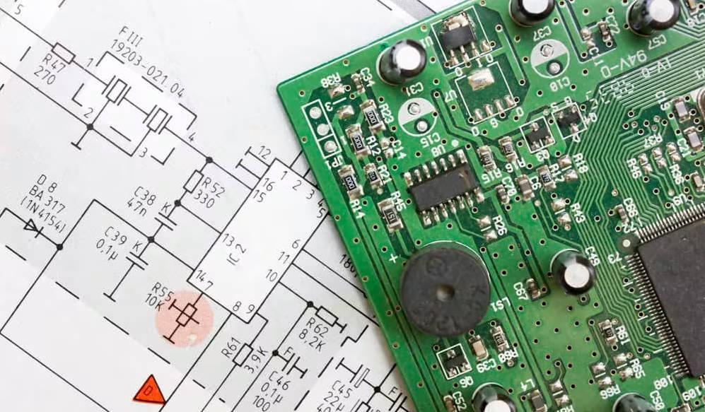
Signal Integrity (SI) in PCB design is the practice of ensuring signals are transmitted cleanly and without distortion from the driver to the receiver. Effective SI is achieved by managing layout strategies to control impedance, minimize reflections, reduce crosstalk, and maintain a stable power delivery network, which is crucial for the performance and reliability of high-speed digital circuits. This comprehensive guide compares different layout strategies, helping you understand the trade-offs and make informed decisions to preserve the quality of your signals.
Table of Contents
- What is Signal Integrity and Why Does It Matter?
- The Groundwork: Fundamental Layout Strategies for SI
- Comparing Trace Routing Strategies: The Arteries of Your PCB
- Tackling Specific SI Problems with Advanced Layout Techniques
- Analysis and Verification: Don’t Guess, Simulate!
- Conclusion: A Holistic Approach to Signal Integrity
What is Signal Integrity and Why Does It Matter?
At its core, signal integrity is a set of measures of the quality of an electrical signal. In an ideal world, a digital signal would be a perfect square wave, transitioning instantly between high and low states. In reality, physical effects of the PCB layout—the traces, vias, and planes—distort this signal. As clock speeds increase and voltage levels decrease, these distortions can lead to system-level failures, including data errors, false clocking, and intermittent glitches. Understanding and actively managing SI is no longer an optional step for specialists; it is a fundamental requirement for any modern electronic design.
Defining Signal Integrity: Beyond a Perfect Square Wave
A “good” signal is one that meets all timing and voltage requirements at the receiver’s input pin. Signal integrity issues manifest as various forms of signal distortion. These include ringing (unwanted oscillation), overshoot/undershoot (voltage levels exceeding or falling below the power rails), and slow signal rise/fall times. Poor SI can cause a ‘1’ to be misinterpreted as a ‘0’ (or vice versa), corrupting data and rendering the device useless. Therefore, SI is about ensuring the signal that arrives is a faithful, timely representation of the signal that was sent.
The High-Speed Challenge: When Does SI Become Critical?
Signal integrity concerns become paramount when the signal’s rise time is comparable to the propagation delay along the trace. A common rule of thumb is that if the trace length is longer than 1/3 of the signal’s rise/fall edge length, it must be treated as a transmission line, and SI effects must be considered. In the past, this applied only to RF or microwave circuits. Today, with rise times in the picosecond range for common interfaces like DDR4, PCIe, and USB 3.0, even short traces on a small board can act as transmission lines, making signal integrity a critical concern for a vast range of digital products.
The Core Enemies of Signal Integrity: A Quick Overview
Four primary issues plague signal integrity, and every layout strategy is designed to combat one or more of them. Understanding these is the first step to creating a robust design.
- Reflections: Caused by impedance mismatches along the signal path (e.g., at connectors, vias, or trace width changes), causing parts of the signal energy to reflect back to the source, distorting the waveform.
- Crosstalk: The unwanted electromagnetic coupling between adjacent traces. The signal in an “aggressor” trace can induce noise in a nearby “victim” trace, potentially causing false switching.
- Power Supply Noise: Also known as Power Integrity (PI) issues, fluctuations on the power and ground rails (due to simultaneous switching of many ICs) can affect signal reference levels, degrading noise margins.
- EMI (Electromagnetic Interference): When a PCB radiates excessive electromagnetic energy, it can interfere with other devices. Conversely, it can also be susceptible to external noise. Good SI practices often lead to good EMI performance.
The Groundwork: Fundamental Layout Strategies for SI
Before a single trace is routed, crucial decisions about component placement, power distribution, and grounding set the stage for good signal integrity. Getting these foundational elements right makes the subsequent routing process significantly easier and more effective.
Strategic Component Placement: The First Line of Defense
Thoughtful component placement is arguably the most critical and cost-effective SI strategy. The goal is to minimize the length of critical high-speed signal paths. Place high-speed components, such as CPUs and memory, as close to each other as possible to reduce trace length, which in turn reduces signal degradation and timing issues. Keep analog and digital sections of the board physically separate to prevent digital noise from corrupting sensitive analog signals. Furthermore, place decoupling capacitors as close as possible to the power and ground pins of every active IC to provide a local source of charge for fast switching events.
The Power Delivery Network (PDN): Fueling Your Signals
A stable Power Delivery Network (PDN) is the bedrock of signal integrity. A signal’s quality is only as good as its reference. The PDN, consisting of power planes, ground planes, and decoupling capacitors, must provide a low-impedance path for current from the power source to the ICs. A poorly designed PDN with high impedance can lead to “ground bounce” and “power rail collapse,” where fast-switching signals cause significant voltage fluctuations. This noise directly impacts the signal’s reference, reducing noise margins and potentially causing logic errors. Using solid power and ground planes, rather than routed power traces, is essential for high-speed designs.
Establishing a Solid Foundation: The Critical Role of Ground Planes
A continuous, solid ground plane is a designer’s best friend for signal integrity. It serves two vital purposes. First, it provides a low-inductance return path for signals. High-frequency currents want to return directly underneath the signal trace; a solid ground plane allows this, minimizing the loop area and thus reducing inductance and EMI radiation. Any split or gap in the ground plane that a high-speed signal must cross will force the return current to find a longer path, creating a large current loop that acts as an antenna and introduces significant impedance discontinuities.
Comparing Trace Routing Strategies: The Arteries of Your PCB
Once the foundation is set, the focus shifts to how signals are routed. The physical geometry and arrangement of traces directly dictate their electrical behavior at high frequencies.
Microstrip vs. Stripline: Which Configuration is Right for Your Design?
Microstrip and stripline are the two most common ways to create controlled-impedance transmission lines on a PCB. The choice between them involves trade-offs in performance, cost, and manufacturability.
- A Microstrip is a trace routed on an outer layer of the PCB, with a solid reference plane (usually ground) directly below it. It is simpler to fabricate and inspect but offers less shielding from noise and radiation.
- A Stripline is a trace routed on an internal layer, sandwiched between two solid reference planes. This configuration provides excellent shielding, resulting in lower emissions and better crosstalk immunity, but it is more complex to manufacture and inspect.
| Feature | Microstrip | Stripline |
|---|---|---|
| Location | Outer PCB layer | Inner PCB layer (between two reference planes) |
| EMI/Shielding | Fair. Prone to radiation and susceptibility. | Excellent. Shielded by two planes, reducing crosstalk and emissions. |
| Propagation Speed | Faster. Signal travels partly through air (lower dielectric constant). | Slower. Signal travels entirely through PCB dielectric material. |
| Fabrication Cost | Lower. Simpler layer stackup. | Higher. More complex stackup and routing on inner layers. |
| Best For | General high-speed routing, cost-sensitive designs. | Very high-speed signals (e.g., clock lines), designs with strict EMI requirements. |
Controlled Impedance Routing: Why Consistency is King
For high-speed signals, a PCB trace must be treated as a transmission line with a specific characteristic impedance (typically 50 ohms for single-ended signals). Controlled impedance is the practice of designing the trace geometry (width, height above the reference plane) and selecting PCB materials to achieve this target impedance. Any variation in impedance along the path—caused by changes in trace width, layer transitions via vias, or gaps in the reference plane—creates a mismatch. These mismatches cause signal reflections, which are a primary source of signal degradation. Maintaining a consistent impedance from driver to receiver is fundamental to preserving signal integrity.
Differential Pair Routing: A Symphony in Symmetry
Differential signaling uses two complementary traces to transmit one signal. The receiver interprets the signal based on the voltage *difference* between the two traces. This technique is highly resilient to common-mode noise because any noise coupled onto the pair will affect both traces equally, leaving the voltage difference unchanged. To achieve this benefit, the two traces must be routed with extreme care:
- Symmetry is key: The two traces should be kept as parallel and as close together as possible throughout their entire length.
- Length matching: The lengths of the two traces must be tightly matched to ensure the signals arrive at the receiver simultaneously, preventing phase differences that can corrupt the signal.
- Consistent impedance: Both the differential impedance (between the two traces) and the common-mode impedance (of each trace to ground) must be controlled.
Any asymmetry in the routing introduces common-mode conversion, where noise begins to affect the differential signal, defeating the purpose of the pair.
Managing Trace Lengths and Skew: Keeping Signals in Sync
In parallel data buses, such as a DDR memory interface, it is critical that all signals in a group arrive at the destination within a specific time window. The difference in arrival time between signals in a group is called skew. Skew is caused by differences in the physical lengths of the traces. PCB designers must use length-matching techniques, often adding serpentine or trombone-like patterns to shorter traces, to equalize the propagation delay across the entire bus. Failure to manage skew can lead to setup and hold time violations at the receiver, resulting in data corruption.
Tackling Specific SI Problems with Advanced Layout Techniques
While fundamental strategies are essential, specific problems often require targeted layout solutions. Understanding which technique to apply is a hallmark of an experienced designer.
How to Tame Reflections: A Comparison of Termination Strategies
Termination is the practice of adding resistors to a transmission line to match the impedance of the driver or receiver, thereby absorbing signal energy and preventing reflections. Several termination strategies exist, each with its own pros and cons.
| Termination Strategy | Description | Pros | Cons |
|---|---|---|---|
| Series Termination | Resistor placed near the driver. | Low power consumption; good for point-to-point topologies. | Slows down signal rise time; not suitable for multiple receivers. |
| Parallel Termination | Resistor placed at the receiver, connected to VCC or GND. | Excellent signal quality; effective at managing reflections. | High constant power consumption. |
| Thevenin Termination | Voltage divider (two resistors) at the receiver. | Very effective; can set the DC bias level. | Highest power consumption; requires two components. |
| AC Termination | Resistor and capacitor in series at the receiver. | No DC power consumption. | Adds delay; requires two components. |
Minimizing Crosstalk: Spacing, Guard Traces, and Orthogonal Routing
Crosstalk is directly related to the proximity of traces. The most effective way to reduce it is to increase the spacing between traces. A common guideline is the “3W rule,” which states that the center-to-center distance between two traces should be at least three times the width of a single trace. For highly sensitive signals, another strategy is to use a guard trace—a trace routed parallel to the signal, grounded at both ends. This guard trace intercepts the electromagnetic fields and shunts the noise to ground. Finally, on adjacent signal layers, routing traces orthogonally (e.g., horizontal traces on one layer, vertical on the next) minimizes the parallel run length between them, significantly reducing broadside coupling.
The Challenge of Vias: Mitigating Discontinuities in High-Speed Design
Vias, which connect traces between different layers, are a necessary evil in complex PCB design. However, they represent significant impedance discontinuities. A via introduces parasitic capacitance and inductance, and the unused portion of a through-hole via, known as a “stub,” can cause severe reflections at high frequencies. To mitigate these effects, designers should minimize the use of vias on critical high-speed lines. When a via is necessary, it is crucial to place ground stitching vias close to the signal via. These provide a low-inductance path for the return current to follow the signal as it changes layers. For extremely high-frequency signals (above 10 GHz), techniques like back-drilling are used to physically remove the unused via stub.
Analysis and Verification: Don’t Guess, Simulate!
In modern high-speed design, relying solely on rules of thumb is not enough. Signal integrity simulation tools allow designers to model the electrical behavior of their PCB layout and predict performance before fabrication, saving costly and time-consuming board respins.
The Role of Pre-Layout and Post-Layout SI Simulation
SI analysis can be performed at two key stages. Pre-layout simulation is done during the schematic phase to explore different layout strategies, determine termination requirements, and define routing constraints before the layout begins. This helps in making high-level decisions, such as choosing the PCB stackup and component placement. Post-layout simulation is performed on the fully routed PCB database. It provides a highly accurate analysis of the final design, allowing for verification of timing, reflections, and crosstalk. This step is essential to catch any violations of the design rules and to ensure the board will function reliably.
Key Metrics to Analyze in an SI Simulation
When running an SI simulation, engineers look at specific metrics to quantify signal quality. The most common tool is the eye diagram, which is generated by overlaying many cycles of a signal. A large, open “eye” indicates a high-quality signal with good noise margin and timing. Other key metrics include measuring overshoot/undershoot, checking for non-monotonic edges, analyzing timing jitter, and quantifying crosstalk noise levels to ensure they are within the receiver’s specified limits.
Conclusion: A Holistic Approach to Signal Integrity
Achieving excellent signal integrity is not about applying a single magic bullet; it is about a holistic and disciplined approach to PCB design. It begins with strategic component placement and a robust PDN design, moves through a careful comparison and implementation of routing strategies like controlled impedance and differential pairing, and is validated by targeted techniques to solve specific issues like reflections and crosstalk. By understanding the fundamental principles and comparing the trade-offs of different layout strategies—from Microstrip vs. Stripline to various termination schemes—designers can build a strong foundation for high-performance, reliable electronic products. In the world of high-speed digital design, a well-thought-out layout is the ultimate key to success.
Signal Integrity, PCB Design, PCB Layout, High-Speed Design, Layout Strategies, what is signal integrity in pcb design, how to improve signal integrity, pcb layout strategies for signal integrity, comparing microstrip vs stripline, differential pair routing best practices, pcb grounding techniques for si, signal integrity analysis, pcb termination strategies, controlled impedance, crosstalk, transmission line, power delivery network (PDN), EMI, PCB simulation

