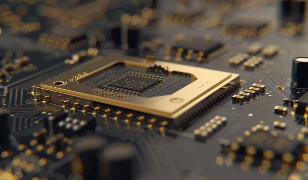
In the golden age of low-speed electronics, a wire was just a wire, and a power plane was just a steady supply of voltage. If the schematic was correct, the board worked. Those days are gone.
As we push data rates beyond 10 Gbps and edge rates into the picosecond range, the physical layout of the Printed Circuit Board (PCB) becomes a complex component in itself. In this regime, two invisible forces dictate the success or failure of your design: Signal Integrity (SI) and Power Integrity (PI).
While often treated as separate disciplines—handled by different simulation tools or even different engineers—they are physically intertwined. A collapse in your power delivery network (PDN) can destroy your signal timing (Jitter), and poor signal routing can inject noise back into your power planes.
This comprehensive guide provides a side-by-side analysis of SI and PI, breaking down the physics, the enemies, the solutions, and the critical intersection where designs often fail.
I: The Fundamentals – Defining the Two Pillars
To master high-speed design, we must first clearly distinguish the objectives of these two disciplines.
1. What is Signal Integrity (SI)?
Signal Integrity is the science of maintaining the quality of an electrical signal as it travels from a transmitter (Tx) to a receiver (Rx).
- The Physics: It treats PCB traces not as wires, but as Transmission Lines.
- The Goal: To ensure that the digital “1” sent by the Tx looks like a “1” when it arrives at the Rx, with correct timing and voltage levels.
- The Domain: Primarily the Time Domain (rise times, flight times) and high-frequency AC Physics.
2. What is Power Integrity (PI)?
Power Integrity is the science of delivering clean, stable voltage to the active components on the PCB, regardless of how fast they switch.
- The Physics: It treats power and ground planes as a Resonant Cavity and a complex R-L-C network.
- The Goal: To maintain a low impedance path from the Voltage Regulator Module (VRM) to the transistor, ensuring $V_{dd}$ stays within tolerance (e.g., ±5%).
- The Domain: Spans from DC (0 Hz) to Gigahertz frequencies.
The High-Level Comparison Matrix
| Feature | Signal Integrity (SI) | Power Integrity (PI) |
| Primary Objective | Data Fidelity (Quality of bits). | Energy Delivery (Stability of Voltage). |
| Key Metric | Bit Error Rate (BER), Eye Opening. | Target Impedance ($Z_{target}$), Voltage Ripple. |
| Main Physical Enemy | Impedance Mismatch, Crosstalk. | Inductance (Loop Inductance), Resonance. |
| Critical Components | Traces, Connectors, Vias. | VRMs, Capacitors, Power Planes. |
| Simulation Output | Eye Diagrams, S-Parameters ($S_{11}, S_{21}$). | Impedance vs. Frequency Plots, DC Drop Maps. |
| Google Featured Snippet | Signal Integrity deals with the quality of the signal path (traces), ensuring data arrives without distortion. Power Integrity deals with the stability of the power distribution network (PDN), ensuring chips receive constant voltage despite rapid current changes. |
II: Deep Dive into Signal Integrity (SI)
When a signal travels fast enough that the length of the trace is greater than 1/10th of the signal’s wavelength, transmission line effects dominate. Here are the three pillars of SI failure.
1. Reflection and Impedance Matching

2. Crosstalk (The Noisy Neighbor)
Crosstalk occurs when electromagnetic energy couples from an “Aggressor” trace to a “Victim” trace. This happens via two mechanisms:
- Capacitive Coupling: The electric field changes, injecting current into the victim.
- Inductive Coupling: The magnetic field changes, inducing voltage on the victim.
There are two types of crosstalk:
- Near-End Crosstalk (NEXT): Noise measured at the transmitter end.
- Far-End Crosstalk (FEXT): Noise that travels along with the signal to the receiver.
- The Fix: The 3W Rule. The distance between trace centers should be at least 3 times the trace width ($W$). For differential pairs, spacing should be even larger.
3. Attenuation and Loss (Dielectric vs. Skin Effect)
As frequencies hit the GHz range, the signal loses energy as it travels.
- Skin Effect: At high frequencies, current flows only on the outer “skin” of the copper. This decreases the effective cross-sectional area, increasing resistance.
- Dielectric Loss: The PCB material (FR-4) absorbs energy as the dipoles in the epoxy try to align with the oscillating field.
- The Fix: Use low-loss materials (like Panasonic Megtron 6 or Rogers RO4350B) and smoother copper foil (HVLP) to reduce insertion loss.
III: Deep Dive into Power Integrity (PI)
While SI focuses on lines, PI focuses on Planes. The goal of PI is to create a Power Distribution Network (PDN) that looks like a low-value resistor across a huge frequency range.
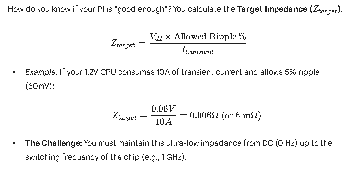
1. The Concept of Target Impedance
2. The Frequency Spectrum of the PDN
Designing a PDN is like conducting an orchestra; different components handle different frequencies.
- DC to 1 kHz (The Regulator): The Voltage Regulator Module (VRM) handles slow changes in load.
- Failure Mode: IR Drop. If copper planes are too thin, resistance causes voltage to sag before it reaches the chip.
- 1 kHz to 1 MHz (Bulk Capacitors): Large Tantalum or Electrolytic caps (47µF – 330µF) store energy to support the VRM.
- 1 MHz to 100 MHz (Decoupling Capacitors): Ceramic MLCCs (0.1µF, 1µF) placed close to the chip.
- Critical Physics: It’s not just about capacitance (C). It’s about Equivalent Series Inductance (ESL). A capacitor stops acting like a capacitor at its Self-Resonant Frequency (SRF). Above this frequency, it becomes an inductor.
- 100 MHz to GHz (Plane Capacitance): Above 100 MHz, discrete capacitors are too slow (too much inductance). We rely on the inter-plane capacitance formed by the Power and Ground planes sandwiching the dielectric.
- The Fix: Use ultra-thin dielectrics (e.g., 2-3 mil thickness) between Layer 2 (GND) and Layer 3 (PWR).
3. The Silent Killer: Loop Inductance
In PI, Inductance (L) is the enemy.
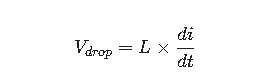
When a processor wakes up, $di/dt$ (change in current over time) is massive. Even a tiny inductance ($L$) creates a massive voltage drop.
- Design Rule: Place capacitors as close to the pin as possible to minimize the loop area. Use “Via-in-Pad” technology to eliminate trace inductance.
IV: The Intersection – Where PI Kills SI
This is the most critical section for advanced designers. Often, a board fails not because of bad SI or bad PI, but because of the interaction between them.
1. Simultaneous Switching Noise (SSN) / Ground Bounce
Imagine a 64-bit data bus switching from “00…00” to “11…11” instantly. All 64 drivers pull current from the power rail and dump it into the ground rail simultaneously.
If the return path (Ground) has inductance, the ground potential at the chip momentarily spikes up (bounces) relative to the board ground.
- The Result: The logic “Low” level rises above the threshold, causing false triggering on quiet lines. This is a PI problem causing an SI failure.
2. The “Return Path” Myth
SI Engineers often focus on the signal trace. But current moves in a loop. The return current travels on the reference plane directly underneath the signal trace.
- The Trap: What happens if a signal trace transitions from Layer 1 to Layer 4?
- If Layer 2 is Ground and Layer 3 is Power, the return current must jump from the Ground plane to the Power plane to follow the signal.
- How does AC current jump between DC planes? It can only pass through a Decoupling Capacitor.
- The Failure: If there is no decoupling capacitor near that via transition, the return current must wander across the board to find the nearest capacitor. This large loop creates a massive magnetic field, causing EMI and Crosstalk.
- The Fix: Place “Stitching Capacitors” or Stitching Vias (if Ground-to-Ground) next to every high-speed signal via.
3. Power Supply Induced Jitter (PSIJ)
Digital buffers are powered by voltage rails. The propagation delay of a logic gate is dependent on its supply voltage.
- Scenario: If the PI is poor and the voltage rail ripples by 50mV.
- Effect: When voltage is low, the transistor switches slower. When voltage is high, it switches faster.
- Outcome: The signal edges arrive at different times. This modulation of timing is called Jitter. No amount of trace routing can fix this; only fixing the PDN can.
V: Simulation and Measurement Methodologies
How do we prove our design works? The tools for SI and PI are distinct.
Signal Integrity Tools
- Time Domain Reflectometry (TDR): Sends a pulse down the line and listens for reflections. It essentially maps impedance over distance.
- Use: Locating a bad connector or a crushed cable.
- The Eye Diagram: A composite overlay of thousands of bits.
- Open Eye: Good signal quality.
- Closed Eye: Excessive Jitter or Noise.
- IBIS Models: (Input/Output Buffer Information Specification). These are behavioral models provided by chip vendors (like Intel or TI) to simulate how the driver behaves.
Power Integrity Tools
- DC Drop Analysis: A simulation that creates a “thermal map” of voltage density. Ideally, you want to see a uniform color (voltage) across the plane.
- AC Impedance Analysis: A frequency sweep plot.
- Goal: To flatten the curve. You want to squash any high-Q resonant peaks where the impedance spikes above the Target Impedance.
- Vector Network Analyzer (VNA): The hardware tool used to measure the impedance of the PDN on a physical prototype.
VI: The Master Design Checklist
To ensure first-pass success in 2025-era designs, use this integrated checklist.
Stack-up & Materials
- [ ] Symmetrical Build: Is the stack-up balanced to prevent warping?
- [ ] Tight Coupling: Are Signal layers adjacent to solid Ground planes?
- [ ] Inter-plane Capacitance: Are Power and Ground planes spaced closely (< 3 mils) for high-frequency PI?
- [ ] Material Selection: Have you chosen a low-loss dielectric (e.g., Rogers, Megtron) for signals > 5 GHz?
Signal Integrity (SI)
- [ ] Impedance Control: Are all single-ended (50Ω) and differential (100Ω/85Ω) traces verified?
- [ ] Length Matching: Are differential pairs length-matched within tolerance (e.g., < 5 mils)?
- [ ] Crosstalk Control: Is the spacing between high-speed busses at least 3W?
- [ ] Via Management: Have back-drills been applied to critical vias to remove stubs?
Power Integrity (PI)
- [ ] IR Drop: Is the DC voltage drop from source to load < 2%?
- [ ] Decoupling Strategy: Is there a capacitor placed at every power pin of the FPGA/MCU?
- [ ] Mounting Inductance: Are capacitors connected with short, wide traces and multiple vias?
- [ ] Target Impedance: Does the simulated PDN impedance stay below $Z_{target}$ up to the Nyquist frequency?
VII: Conclusion
In high-speed PCB design, Signal Integrity and Power Integrity are two sides of the same coin. You cannot have a clean signal without stable power, and you cannot have stable power without managing the noise generated by high-speed signals.
- SI is about geometry, termination, and materials. It protects the data.
- PI is about capacitance, inductance, and low-impedance paths. It protects the stability.
For the modern engineer, the days of “connect the dots” are over. Successful design now requires a holistic view where the schematic, the stack-up, and the layout are all engineered to respect the laws of physics at GHz frequencies.
Whether you are designing a 5G base station or an automotive radar system, the winners will be those who respect the “Two Pillars” equally.

