The choice between a single-layer and a multi-layer Printed Circuit Board (PCB) is a fundamental decision in electronic design that directly impacts cost, performance, and form factor. Single-layer PCBs are the optimal choice for simple, low-density, and budget-conscious applications, while multi-layer PCBs are essential for complex, high-performance electronics where space and signal integrity are critical. Understanding the trade-offs between these two options is the key to a successful and cost-effective product.
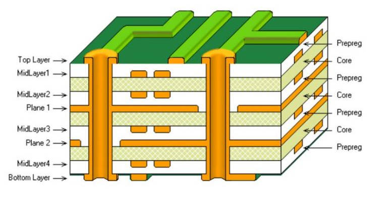
Table of Contents
- What is a Printed Circuit Board (PCB)?
- Understanding Single-Layer PCBs: The Foundation of Electronics
- Exploring Multi-Layer PCBs: The Power of Density
- Head-to-Head Comparison: Single-Layer vs. Multi-Layer PCB
- How to Choose: Key Factors for Your Design Decision
- What About Double-Sided PCBs? The Middle Ground
- Final Verdict: Matching the PCB to the Project
What is a Printed Circuit Board (PCB)?
Before diving into the single vs. multi-layer debate, it’s crucial to understand what a PCB is. A Printed Circuit Board is the foundational bedrock of modern electronics. It’s a rigid or flexible board made of a non-conductive substrate material, with conductive pathways, or “traces,” etched or printed onto it. These traces connect different electronic components (like resistors, capacitors, and integrated circuits) that are soldered to the board, allowing them to function together as a single, cohesive circuit. The PCB replaces the old, cumbersome method of point-to-point wiring, enabling the creation of compact, reliable, and mass-producible electronic devices.
Understanding Single-Layer PCBs: The Foundation of Electronics
A single-layer PCB, also known as a single-sided PCB, is the most basic and common type of circuit board. As its name implies, it consists of a single layer of conductive material, typically copper, on one side of a non-conductive substrate. All electronic components are mounted on one side, and the entire network of conductive traces resides on the other. This simplicity is both its greatest strength and its most significant limitation.
Anatomy of a Single-Layer Board
A single-layer PCB is constructed from four primary materials laminated together:
- Substrate: The base material, typically FR-4 (a fiberglass-epoxy composite), which provides rigidity and electrical insulation.
- Copper Layer: A thin foil of copper is laminated onto the substrate. This is the layer that is etched to create the traces that connect the components.
- Solder Mask: A thin, polymer layer (usually green) applied over the copper traces to prevent oxidation and to stop solder bridges from forming between closely spaced solder pads during assembly.
- Silkscreen: An ink layer applied on top of the solder mask to add labels, component designators, and other human-readable information, which aids in assembly and troubleshooting.
The Clear Advantages of Simplicity
The primary appeal of single-layer boards lies in their simplicity, which translates into several key benefits. First and foremost is cost. With fewer manufacturing steps and less material, they are significantly cheaper to design, prototype, and produce in mass quantities. The design process itself is more straightforward, making it ideal for beginners or projects with tight deadlines. Furthermore, troubleshooting and repairs are much easier because all components and traces are visible and accessible from one side.
Limitations and When to Look Elsewhere
However, the simplicity of a single-layer PCB introduces major constraints. The most significant challenge is circuit density and routing. With all traces confined to a single plane, routing complex circuits without traces crossing is difficult and often impossible. This forces designers to use larger boards or employ jumper wires to complete connections, defeating the purpose of a compact design. This limited routing space also makes single-layer boards more susceptible to signal integrity issues like crosstalk and electromagnetic interference (EMI), as there are no dedicated ground or power planes to provide shielding.
Exploring Multi-Layer PCBs: The Power of Density
A multi-layer PCB is a circuit board that consists of three or more conductive copper layers. These layers are laminated together with insulating materials, appearing as a single, complex board. The inner layers are typically used for routing signals and, crucially, for dedicated power and ground planes. This layered approach overcomes the fundamental limitations of single-layer boards, enabling incredibly dense and high-performance electronic designs.
The Layered Construction Explained
Multi-layer PCBs are essentially a “sandwich” of single or double-sided boards. The construction involves alternating layers of conductive copper and insulating dielectric material. These layers are bonded together under high temperature and pressure. The key components are:
- Cores: These are rigid, double-sided PCBs that form the central part of the stack-up.
- Prepreg: A layer of fiberglass cloth impregnated with epoxy resin. It acts as the “glue” that binds the cores and copper foils together when heated.
- Vias: These are copper-plated holes that drill through the various layers, creating electrical connections between them. There are different types, including through-hole vias (all layers), blind vias (outer to inner), and buried vias (inner to inner).
The Unmistakable Advantages of Complexity
The primary benefit of multi-layer PCBs is a massive increase in component density. By routing traces on multiple inner layers, designers can create much smaller and lighter devices. A circuit that would require a large single-layer board can be condensed into a compact multi-layer design, which is essential for modern devices like smartphones and wearables. Furthermore, the inclusion of dedicated ground and power planes dramatically improves signal integrity. These planes act as a shield, reducing EMI, and provide a stable voltage reference, which is critical for high-speed digital circuits. This leads to better performance, higher reliability, and improved power distribution across the board.
The Inherent Trade-offs and Costs
The sophistication of multi-layer PCBs comes with significant trade-offs. The most obvious is the cost. The complex manufacturing process, additional materials, and tighter tolerances make them substantially more expensive than their single-layer counterparts. Design complexity also increases exponentially; managing layer stack-up, impedance control, and via placement requires more expertise and advanced design software. Finally, repair and troubleshooting become much more difficult, as inner-layer traces are inaccessible. Any flaw in an inner layer often means the entire board must be scrapped.
Head-to-Head Comparison: Single-Layer vs. Multi-Layer PCB
To make the decision clearer, here is a direct comparison of the key attributes of single-layer and multi-layer PCBs.
| Attribute | Single-Layer PCB | Multi-Layer PCB |
|---|---|---|
| Cost | Low | High |
| Design Complexity | Simple and straightforward | Complex, requires expertise in layer stack-up and signal integrity |
| Component Density | Low | Very High |
| Board Size | Larger for a given circuit complexity | Smaller and more compact |
| Performance & Signal Integrity | Lower; susceptible to noise and crosstalk | Higher; dedicated ground/power planes provide excellent EMI shielding |
| Manufacturing Time | Short lead times | Longer lead times due to lamination and drilling processes |
| Typical Applications | Calculators, toys, power supplies, simple sensors, LED lighting | Smartphones, computers, medical devices, aerospace systems, IoT devices |
How to Choose: Key Factors for Your Design Decision
Which type of PCB is better for your design? The answer depends entirely on your project’s specific requirements. Ask yourself the following questions to guide your decision.
Circuit Complexity and Component Density
This is the most critical factor. How many components does your circuit have? How many connections are there between them? If you are designing a simple circuit with a handful of components and straightforward connections, a single-layer PCB is likely sufficient. However, if your design involves microcontrollers, dense BGA packages, or a large number of interconnected components, the routing challenges will almost certainly necessitate a multi-layer PCB to manage the complexity and avoid a sprawling, inefficient layout.
Budget and Manufacturing Costs
What is your budget for prototyping and production? For hobbyist projects, educational purposes, or extremely cost-sensitive consumer products, the low cost of a single-layer PCB is a decisive advantage. The price difference is not trivial; a multi-layer board can be several times more expensive per unit. If your product’s success hinges on minimizing production costs, you must justify the added expense of a multi-layer board with a clear performance or size requirement.
Size Constraints and Form Factor
How large can your final product be? If you are designing a device where space is at a premium—such as a smartwatch, a compact sensor, or a handheld gadget—a multi-layer PCB is the only practical option. The ability to stack traces and components vertically allows for a dramatic reduction in the board’s footprint. If size is not a constraint and you have ample room for a larger board, a single-layer PCB could be a viable, cost-effective choice.
Performance and Signal Integrity Requirements
What are the operational demands of your circuit? If your design involves high-frequency signals (e.g., RF, high-speed data buses), then signal integrity is paramount. A multi-layer PCB with dedicated ground and power planes is essential for providing controlled impedance, minimizing crosstalk between traces, and shielding against external noise. For low-frequency, low-power applications where these issues are negligible, a single-layer PCB will perform adequately.
What About Double-Sided PCBs? The Middle Ground
It’s important to mention a third option: the double-sided PCB. This board has conductive copper layers on both the top and bottom of the substrate. This provides more routing flexibility than a single-layer board without the full cost and complexity of a multi-layer design. Components can be mounted on both sides, increasing density. A double-sided PCB is an excellent compromise for moderately complex circuits where a single layer is too restrictive, but a four-layer board would be overkill and too expensive.
Final Verdict: Matching the PCB to the Project
Ultimately, there is no single “better” type of PCB. The superior choice is the one that best aligns with your project’s constraints and goals. A single-layer PCB is the undisputed champion for simple, low-cost electronics where performance and size are not primary concerns. It represents the most economical and straightforward path from design to a functional product. Conversely, a multi-layer PCB is the necessary and powerful solution for the complex, compact, and high-performance devices that define modern technology. By carefully evaluating your design’s complexity, budget, size, and performance needs, you can confidently select the right foundation for your electronic innovation.
Single-Layer vs Multi-Layer PCBs, which pcb is better, single-layer pcb, multi-layer pcb, printed circuit board design, advantages of multi-layer pcb, disadvantages of single-layer pcb, how to choose a pcb, pcb design factors, pcb cost comparison, single-sided vs multi-sided pcb, pcb layer stackup, what is a single-layer pcb, what is a multi-layer pcb

