Sustainable PCB manufacturing involves adopting eco-friendly materials, energy-efficient processes, and end-of-life management strategies to minimize the environmental impact of printed circuit boards. This green shift addresses the hazardous waste from traditional methods by championing alternatives like biodegradable substrates (e.g., cellulose, lignin), lead-free solders mandated by RoHS, and additive manufacturing techniques that drastically reduce chemical and material waste. By comparing these green alternatives, manufacturers can navigate the path toward a more sustainable and circular electronics industry.
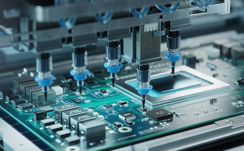
Table of Contents
- The Environmental Imperative: Why Traditional PCB Manufacturing Needs a Green Revolution
- What is Sustainable PCB Manufacturing? A Holistic Approach
- Green Alternatives Compared: A Deep Dive into Sustainable Materials
- Reinventing the Process: Eco-Friendly Fabrication & Assembly Techniques
- Lifecycle Management: Designing for Disassembly and the Circular Economy
- The Business Case: What are the Benefits and Challenges of Going Green?
- The Future is Green: What’s Next for Sustainable Electronics?
- Frequently Asked Questions (FAQ)
The Environmental Imperative: Why Traditional PCB Manufacturing Needs a Green Revolution
The ubiquitous printed circuit board is the nervous system of modern electronics, yet its traditional manufacturing process casts a long and dark environmental shadow. For decades, the industry has relied on methods that are resource-intensive, energy-consuming, and heavily dependent on hazardous materials. The push for sustainability is not merely a trend but a critical necessity driven by regulatory pressure, consumer awareness, and the undeniable reality of electronic waste (e-waste) overwhelming global recycling systems. Understanding the shortcomings of the conventional approach is the first step toward appreciating the value and urgency of adopting greener alternatives.
The Hazardous Footprint of Conventional PCBs
At the core of a traditional PCB is the FR-4 substrate, a composite of woven fiberglass cloth with an epoxy resin binder that is flame-retardant (hence “FR”). While effective and inexpensive, its production and disposal are problematic. The epoxy resins often contain brominated flame retardants (BFRs), which can release toxic dioxins and furans when incinerated improperly. Furthermore, the fabrication process is subtractive, meaning it starts with a copper-clad laminate and etches away unwanted copper using harsh chemical solutions like ferric chloride or ammonium persulfate. This process generates significant quantities of toxic chemical sludge that requires specialized and costly treatment. The use of lead-based solder, a potent neurotoxin, was standard practice for decades, leading to widespread environmental contamination during disposal.
From Cradle to Grave: The Unsustainable Lifecycle of Electronics
The environmental impact of a PCB extends far beyond its factory origins. The lifecycle is linear: take, make, dispose. Raw materials are extracted, processed with significant water and energy inputs, assembled into a product with a short lifespan, and then discarded. This creates a mountain of e-waste, which is the world’s fastest-growing domestic waste stream. When PCBs end up in landfills, the heavy metals they contain—including lead, mercury, and cadmium—can leach into the soil and groundwater, posing severe risks to ecosystems and human health. The complex, bonded nature of FR-4 and its components makes recycling difficult and economically unviable, meaning valuable materials like copper, gold, and silver are often lost forever.
What is Sustainable PCB Manufacturing? A Holistic Approach
Sustainable PCB manufacturing is a comprehensive philosophy that reimagines the entire product lifecycle to minimize environmental harm. It is not about a single change but a multi-faceted strategy that integrates eco-friendly practices from the initial design concept to end-of-life recycling. The goal is to move away from the linear “take-make-dispose” model and toward a circular economy, where resources are kept in use for as long as possible. This approach requires innovation in materials science, process engineering, and product design, all working in concert to create electronics that are as responsible as they are revolutionary.
Beyond Materials: The Three Pillars of Green PCB Production
True sustainability in PCB production rests on three interconnected pillars:
- Sustainable Materials: This involves replacing hazardous or non-renewable materials with greener alternatives. Key areas of focus include developing biodegradable or recyclable substrates to replace FR-4, using halogen-free flame retardants, and mandating the use of lead-free solders and surface finishes.
- Eco-Friendly Processes: This pillar targets the manufacturing stage itself. It includes reducing water and energy consumption, implementing closed-loop systems to recycle chemical etchants, and adopting additive manufacturing techniques (like 3D printing) that build circuits layer-by-layer, virtually eliminating waste.
- Lifecycle Management: This considers the entire life of the PCB, from cradle to grave and back to cradle. It emphasizes Design for Environment (DfE) principles, making boards easier to disassemble, repair, and recycle. It also involves establishing robust take-back programs and developing advanced recycling technologies to recover valuable materials efficiently.
Green Alternatives Compared: A Deep Dive into Sustainable Materials
The substrate is the foundation of a PCB, and the shift away from conventional FR-4 is a cornerstone of the green electronics movement. Researchers and manufacturers are exploring a wide array of innovative materials, each with a unique profile of performance, cost, and environmental benefits. The ideal green substrate is not only biodegradable or easily recyclable but also meets the stringent electrical and thermal performance requirements of modern electronics. This section compares some of the leading contenders vying to become the new industry standard.
The Substrate Showdown: Moving Beyond FR-4
The dominance of FR-4 is due to its low cost, excellent insulation properties, and mechanical robustness. However, its non-biodegradable nature and reliance on brominated flame retardants make it a primary target for replacement. The alternatives range from natural-fiber composites to high-performance polymers.
Bio-based Substrates are a promising category derived from renewable resources like cellulose, lignin, flax, or even banana fibers. These materials offer excellent biodegradability, reducing landfill burden. While their electrical performance, particularly at high frequencies, may not yet match high-grade FR-4, they are increasingly suitable for low-to-mid-range applications like consumer electronics and IoT devices. Their primary challenge lies in moisture absorption and thermal stability, though ongoing research is rapidly closing this gap.
Paper-Based PCBs (e.g., CEM-1, FR-2) have been used for decades in single-sided, low-cost applications. While an improvement over fiberglass, they are now being reinvented with more sustainable resins and manufacturing processes. They offer a low-cost, lightweight alternative for simple circuits but lack the multi-layer capability and mechanical strength of FR-4.
Liquid Crystal Polymers (LCPs) represent a high-performance green alternative. LCPs are halogen-free, exhibit excellent high-frequency electrical properties (low dielectric loss), and have very low moisture absorption, making them ideal for demanding applications like RF/microwave circuits and medical devices. While not biodegradable, they are highly recyclable. The main barrier to widespread adoption is their significantly higher cost compared to FR-4.
Comparison of PCB Substrate Materials
| Material | Key Characteristics | Environmental Impact | Performance | Best For |
|---|---|---|---|---|
| FR-4 (Epoxy/Glass) | Industry standard, low cost, robust. | Non-biodegradable, often contains halogens, energy-intensive. | Excellent all-around electrical and thermal performance. | General-purpose electronics, multi-layer boards. |
| Bio-based (Cellulose, Flax) | Renewable source, lightweight. | Biodegradable, low carbon footprint. | Good for low/mid-frequency; improving thermal stability. | Disposable electronics, IoT, consumer goods. |
| Paper-Based (Phenolic) | Very low cost, easy to punch/drill. | More biodegradable than FR-4 but uses phenolic resins. | Limited to single-layer, lower electrical performance. | Toys, calculators, single-sided consumer electronics. |
| Liquid Crystal Polymer (LCP) | Excellent RF performance, flexible, low moisture absorption. | Halogen-free, highly recyclable, but high cost. | Superior for high-frequency and high-speed digital. | 5G antennas, medical implants, aerospace. |
Reinventing the Process: Eco-Friendly Fabrication & Assembly Techniques
A truly sustainable PCB is not just made from green materials; it is made through green processes. The traditional subtractive manufacturing method is inherently wasteful. Innovations in fabrication and assembly are now targeting this inefficiency, aiming to reduce chemical use, conserve resources, and eliminate harmful substances from the production line entirely.
How Can We Make PCB Etching Greener?
The subtractive etching process is one of the most chemically intensive steps in PCB fabrication. Greener approaches focus on two main areas: chemistry and conservation. This includes developing alternative etchants that are less toxic and more easily regenerated. More importantly, manufacturers are implementing closed-loop regeneration systems that continuously reclaim and reuse etching chemicals, drastically reducing the output of hazardous liquid waste. These systems not only cut down on pollution but also offer significant cost savings by reducing the need to purchase fresh chemicals and pay for waste disposal.
The Rise of Additive Manufacturing: Printing Circuits, Not Wasting Copper
Additive manufacturing represents a paradigm shift from the wasteful subtractive model. Instead of etching away copper, these techniques build the conductive traces directly onto the substrate, layer by layer. Methods like inkjet printing and aerosol jet printing precisely deposit conductive inks (containing nano-particles of silver or copper) only where they are needed. The benefits are immense:
- Waste Reduction: It virtually eliminates copper and chemical etchant waste, with material usage efficiency approaching 98%.
- Water & Energy Savings: It bypasses the multiple chemical bath and rinsing steps of traditional fabrication, saving vast amounts of water and energy.
- Design Flexibility: It allows for the creation of complex, 3D circuits on flexible or unconventional substrates, opening doors for innovative product designs.
While still maturing for high-volume, high-density applications, additive manufacturing is rapidly becoming the go-to method for prototyping and specialized electronics.
The RoHS Revolution: The Impact and Importance of Lead-Free Soldering
The European Union’s Restriction of Hazardous Substances (RoHS) directive, first enacted in 2006, was a landmark piece of legislation that catalyzed a global shift in PCB assembly. Its primary mandate was the elimination of six hazardous substances, most notably lead in solder. This forced the industry to adopt lead-free solder alloys, typically composed of tin, silver, and copper (SAC). The transition was challenging, as lead-free solders have higher melting points (requiring more energy) and different mechanical properties. However, it has been a resounding success in reducing the amount of toxic lead entering the waste stream, protecting both environmental and human health. The RoHS directive proves that regulation can be a powerful driver of sustainable innovation.
Lifecycle Management: Designing for Disassembly and the Circular Economy
The final frontier of sustainable PCB manufacturing is to address what happens to the product after it leaves the consumer’s hands. A circular economy model for electronics is one where waste is designed out of the system. This requires a fundamental shift in thinking, where designers and engineers plan for a product’s end-of-life from the very beginning.
What is Design for Environment (DfE)?
Design for Environment (DfE) is a proactive design methodology that integrates environmental considerations into every phase of product development. For PCBs, this means making conscious choices to enhance sustainability. Key DfE principles include:
- Design for Disassembly: Using modular designs, and avoiding strong adhesives or potting compounds that make it impossible to separate components from the board.
- Material Selection: Prioritizing recycled and recyclable materials and clearly labeling plastic components to aid in sorting.
- Component Reduction: Minimizing the number of components and materials used to simplify the recycling process.
- Energy Efficiency: Designing circuits that consume less power during their operational life.
Closing the Loop: Strategies for PCB Recycling and Component Recovery
Effective recycling is crucial for closing the resource loop. Traditional e-waste recycling often involves crude methods like shredding and incineration, which are inefficient and polluting. Advanced recycling techniques are now emerging, such as hydrometallurgy and pyrometallurgy, which use chemical and high-temperature processes to recover a higher percentage of precious metals like gold, silver, palladium, and copper from crushed PCBs. Furthermore, designing boards for component recovery allows valuable integrated circuits and other parts to be harvested and reused, extending their useful life and reducing the demand for new manufacturing.
The Business Case: What are the Benefits and Challenges of Going Green?
Adopting sustainable practices is not just an ethical obligation; it is increasingly a smart business strategy. While there are initial hurdles to overcome, the long-term benefits often outweigh the costs, creating a powerful competitive advantage in a world that values corporate responsibility.
Advantages: More Than Just Good PR
The move toward sustainable PCB manufacturing offers a multitude of tangible benefits. It ensures compliance with a growing list of international regulations like RoHS and WEEE (Waste Electrical and Electronic Equipment), avoiding costly fines and market access restrictions. It can lead to significant cost savings through reduced material waste, lower energy and water consumption, and decreased fees for hazardous waste disposal. Perhaps most importantly, a strong environmental commitment enhances brand reputation, attracting environmentally conscious customers and top-tier engineering talent who want to work for forward-thinking companies.
Hurdles to Overcome: Navigating the Challenges of Adoption
Despite the clear benefits, the transition to green manufacturing is not without its challenges. The initial capital investment for new equipment, such as additive manufacturing systems or closed-loop chemical recyclers, can be substantial. Some green materials may not yet offer the same level of performance or reliability as their traditional counterparts, requiring extensive testing and validation. The supply chain for novel bio-based substrates may also be less mature and more expensive than the well-established FR-4 market. Overcoming these hurdles requires a strategic, long-term commitment from leadership and a culture of continuous innovation.
The Future is Green: What’s Next for Sustainable Electronics?
The trajectory for PCB manufacturing is unequivocally green. The future will see the rise of even more innovative solutions that push the boundaries of what is possible. Research into transient electronics—circuits designed to completely and harmlessly dissolve in water after a set period—could revolutionize medical implants and environmental sensors. The integration of Artificial Intelligence (AI) and machine learning will optimize manufacturing processes for minimal energy and resource use. As material science advances, we can expect to see biodegradable substrates that match or even exceed the performance of FR-4, making sustainability the default, not the alternative. The ultimate goal is a fully circular electronics industry where every component is designed to be reused, remanufactured, or returned safely to the biosphere.
Frequently Asked Questions (FAQ)
Are green PCBs as reliable as traditional FR-4 boards?
Reliability depends on the specific alternative and application. High-performance green materials like LCPs can exceed the reliability of FR-4 in demanding RF applications. While some emerging bio-based substrates may have limitations in extreme temperatures or high-moisture environments, they are often perfectly reliable for a wide range of consumer and industrial electronics. Rigorous testing and qualification are key to ensuring a green PCB meets the required performance standards for its intended use.
How much more do sustainable PCBs cost?
The cost varies significantly. Simple changes like switching to RoHS-compliant lead-free solder have become cost-neutral. However, advanced substrates like LCPs can be substantially more expensive than FR-4. Conversely, processes like additive manufacturing can reduce overall costs by minimizing material waste, despite a higher initial equipment investment. As technology matures and economies of scale grow, the cost of many green alternatives is expected to become competitive with traditional methods.
What is the RoHS directive?
RoHS stands for the Restriction of Hazardous Substances. It is a directive from the European Union that restricts the use of specific hazardous materials found in electrical and electronic products. The substances restricted include lead, mercury, cadmium, hexavalent chromium, polybrominated biphenyls (PBB), and polybrominated diphenyl ethers (PBDE). Compliance is mandatory for most electronic products sold in the EU and has become a de facto global standard.
Can any PCB manufacturer produce eco-friendly boards?
Not all manufacturers have the capabilities or certifications to produce a full range of eco-friendly PCBs. While most can handle RoHS-compliant assembly, producing boards with specialized substrates (like LCP or bio-polymers) or using advanced techniques like additive manufacturing requires specific expertise and equipment. It is essential to partner with a manufacturer who can demonstrate a clear commitment to sustainability and provide data on their materials, processes, and waste management practices.
Sustainable PCB manufacturing, green PCB, eco-friendly PCB, biodegradable PCB substrate, environmental impact of PCB fabrication, lead-free PCB assembly, additive manufacturing for printed circuit boards, RoHS directive, FR-4 alternatives, green electronics, circular economy in electronics, Design for Environment (DfE), e-waste reduction, sustainable electronics manufacturing

