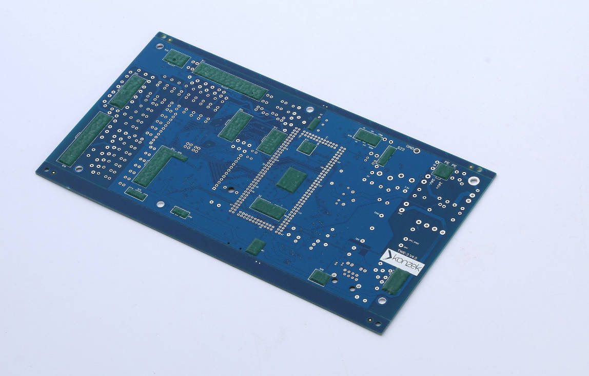
High-Speed Printed Circuit Boards (PCBs) are the critical hardware foundation enabling the unprecedented speed, bandwidth, and low latency of 5G networks and modern data centers. As data rates surge into the multi-gigabit and even terabit per second range, these are not your standard circuit boards; they are highly engineered marvels designed to maintain signal integrity against immense physical challenges. Understanding their role involves delving into the demanding applications, the complex design hurdles like signal integrity and thermal management, and the revolutionary materials required to make our hyper-connected world a reality.
Table of Contents
- Why Are High-Speed PCBs the Unsung Heroes of 5G and Data Centers?
- Key High-Speed PCB Applications: Where Do They Make a Difference?
- The Triple Threat: Overcoming Critical High-Speed PCB Design Challenges
- The Material Revolution: Moving Beyond Standard FR-4
- Advanced Manufacturing & Design Techniques for High-Speed Success
- The Future is Faster: What’s Next for High-Speed PCBs?
- Conclusion: The Silent Enabler of Our Connected World
Why Are High-Speed PCBs the Unsung Heroes of 5G and Data Centers?
The insatiable global demand for faster data, real-time communication, and massive data processing power is the primary driver behind the evolution of high-speed PCBs. Standard PCBs, typically made from FR-4 material, begin to fail as signal frequencies increase. The electrical properties of the board itself start to distort, attenuate, and corrupt the data it’s meant to carry. High-speed PCBs, therefore, are purpose-built to function as a transparent transmission medium, ensuring that a digital signal at one end of a trace is received identically at the other end, even at staggering speeds of 25 Gbps, 56 Gbps, and beyond.
In the context of 5G technology, this translates to achieving the core promises of the new generation: enhanced Mobile Broadband (eMBB), Ultra-Reliable Low-Latency Communication (URLLC), and Massive Machine-Type Communications (mMTC). For everything from streaming 8K video on a smartphone to enabling autonomous vehicle communication, the signal must travel flawlessly through base station antennas, radios, and processing units—all of which rely on high-speed PCBs. Similarly, in data centers, these advanced boards form the nervous system of servers, switches, and routers. They facilitate the massive “East-West” traffic (server-to-server communication within the data center) and “North-South” traffic (data moving between the data center and the outside world), which is essential for cloud computing, AI model training, and big data analytics.
Key High-Speed PCB Applications: Where Do They Make a Difference?
High-speed PCBs are not a one-size-fits-all solution. Their design, materials, and complexity are tailored to specific applications within the 5G and data center ecosystems. Recognizing these distinct roles is key to understanding the engineering challenges involved.
In 5G Infrastructure: Powering the Wireless Revolution
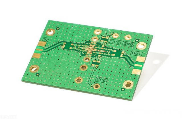
5G infrastructure is a complex network of interconnected components, each with unique PCB requirements. A primary application is in the Active Antenna Units (AAUs) or Remote Radio Units (RRUs). These units combine the antenna array with the radio transceivers and operate at high frequencies, including the Sub-6 GHz and millimeter-wave (mmWave) bands (24 GHz and above). PCBs in AAUs must handle high-frequency RF signals with minimal loss and integrate digital processing components. This often requires *hybrid PCBs* that use specialized, low-loss RF materials for the antenna portion and more conventional materials for the digital control circuits, all on a single, complex board.
Further down the chain are the Baseband Units (BBUs) or Distributed/Centralized Units (DUs/CUs). These are the digital processing powerhouses of the base station. The PCBs here are incredibly dense, high-layer-count boards responsible for routing massive amounts of data between processors, FPGAs, and high-speed optical interfaces. The primary challenge is routing thousands of high-speed differential pairs while maintaining signal integrity and managing the immense heat generated by the powerful processors. These boards are classic examples of high-speed digital design, pushing the limits of trace width, spacing, and via technology.
Inside the Modern Data Center: The Backbone of the Cloud
Within a hyperscale data center, the most prominent application of high-speed PCBs is in the server and switch backplanes. A backplane is a massive PCB that serves as the spine of a chassis, allowing multiple daughter cards (like line cards, server blades, or supervisor engines) to connect and communicate with each other. Modern backplanes can be over 25 layers thick, several feet long, and must support data rates of 56 Gbps to 112 Gbps per channel. Designing a board of this scale to maintain signal integrity across such long distances is one of the pinnacle challenges in PCB engineering.
Another critical application is on the line cards themselves, which plug into the backplane. These boards house the network processors, switch fabrics (ASICs), and optical module interfaces (e.g., QSFP-DD, OSFP). The PCB design here is characterized by extreme density. Signals must be routed from the ASIC BGA package, which can have thousands of pins, to the edge connectors for the backplane and the cages for the pluggable optical modules. This requires advanced techniques like High-Density Interconnect (HDI) and careful impedance control to ensure the data stream remains error-free from the chip all the way to the fiber optic cable.
The Triple Threat: Overcoming Critical High-Speed PCB Design Challenges
Designing a high-speed PCB is a balancing act between three interconnected physical constraints: signal integrity, power integrity, and thermal management. Failure in any one of these domains will lead to system failure, regardless of how well the others are implemented.
Challenge 1: Mastering Signal Integrity (SI) in a High-Frequency World
Signal Integrity (SI) is the measure of the quality of an electrical signal as it travels from a transmitter to a receiver. At high frequencies, the PCB trace is no longer a simple wire but a complex transmission line where various effects can degrade the signal. The primary goal of SI engineering is to minimize these effects. Key concerns include Insertion Loss, which is the total signal power lost as it travels down the trace due to dielectric material absorption and conductor skin effect; Crosstalk, where the signal in one trace electromagnetically couples to and induces noise in an adjacent trace; and Skew, where signals in a differential pair or parallel bus arrive at the receiver at slightly different times, causing timing errors.
Controlling these factors requires meticulous design. This includes precise impedance control (ensuring the trace maintains a consistent characteristic impedance, typically 50 ohms for single-ended or 100 ohms for differential pairs), routing traces with sufficient spacing to minimize crosstalk, and matching the lengths of differential pairs to prevent skew. Sophisticated electromagnetic simulation software is used extensively to model and predict these effects before a single board is ever fabricated, saving countless hours and resources.
| Challenge | Description | High-Speed PCB Solution |
|---|---|---|
| Insertion Loss | Signal strength reduction as it travels along a trace. Worsens significantly with frequency and trace length. | Use of low-loss dielectric materials (low Df), smoother copper foils, and wider traces. |
| Crosstalk | Unwanted signal coupling between adjacent traces, causing noise and errors. | Increase spacing between traces (3W rule), use ground planes for shielding, route on different layers orthogonally. |
| Impedance Mismatch | Discontinuities in impedance cause signal reflections, degrading signal quality (ringing, over/undershoot). | Precise control of trace width, dielectric height, and material (Dk). Avoid stubs, use proper via design. |
| Skew | Timing difference between signals that should arrive simultaneously (e.g., in a differential pair). | Meticulous length-matching of traces, often using serpentine or accordion routing patterns. |
Challenge 2: Ensuring Rock-Solid Power Integrity (PI)
While SI gets much of the attention, Power Integrity (PI) is equally vital. High-speed digital components, like FPGAs and ASICs, have dynamic power demands, drawing large, instantaneous currents when they switch. The PCB’s Power Distribution Network (PDN) must be able to supply this current instantly with minimal voltage drop or noise. A poorly designed PDN can cause voltage rail collapse, leading to logic errors or system resets. It can also be a significant source of electromagnetic interference (EMI) that disrupts signal integrity.
Achieving good PI involves designing the PDN as a low-impedance path from the voltage regulator to the component’s power pins across a wide frequency range. This is accomplished through the strategic use of power and ground planes within the PCB stackup, which act as a large, built-in capacitor. Additionally, a carefully planned array of decoupling capacitors of various sizes are placed as close as possible to the component’s power pins. These capacitors act as local energy reservoirs, supplying the instantaneous current demands that the main power supply cannot respond to quickly enough.
Challenge 3: Taming the Heat with Advanced Thermal Management
High-speed equals high power, and high power equals high heat. The same powerful processors and high-frequency signals that demand advanced SI and PI also generate a tremendous amount of thermal energy. If this heat is not effectively removed, component temperatures can rise beyond their safe operating limits, leading to performance throttling, reduced reliability, and eventual failure. The PCB itself plays a crucial role in the thermal path, acting as the first stage of heat removal from the component.
Several techniques are employed at the PCB level to manage heat. Thermal vias are vias placed directly under or around a hot component, providing a direct thermal path to transfer heat from the top layers of the board to the internal ground or power planes, which act as large heat spreaders. For extreme power applications, heavy copper traces and planes (using copper weights of 3 oz or more, compared to the standard 1 oz) can be used to improve heat conduction across the board. In some designs, metal coins or embedded heat sinks are directly integrated into the PCB fabrication process to provide a highly efficient, localized cooling solution for the most demanding components.
The Material Revolution: Moving Beyond Standard FR-4
Perhaps the most fundamental change in high-speed PCB design is the shift in base materials. Standard FR-4 (Flame Retardant 4), a glass-epoxy laminate, is inexpensive and reliable for low-frequency applications. However, its electrical properties, specifically its dielectric constant (Dk) and dissipation factor (Df), are inadequate for high-speed signals. A high Df (also called loss tangent) means the material absorbs more of the signal’s energy as heat, causing significant insertion loss. An inconsistent Dk can cause impedance variations, leading to reflections. Therefore, 5G and data center applications mandate the use of advanced, low-loss materials.
Low-Loss and Ultra-Low-Loss Laminates: The Foundation of Speed
To combat signal loss, the industry has turned to a new class of PCB laminates engineered for high-frequency performance. These materials are characterized by their very low and stable Dk and Df values across a wide frequency range. Popular material families include those from manufacturers like Rogers Corporation (e.g., RO4000 series), Panasonic (e.g., Megtron 6, Megtron 7), and Isola (e.g., Tachyon 100G). These materials use specialized resin systems and flatter glass weaves to minimize the factors that contribute to signal loss at high frequencies.
Choosing the right material is a trade-off between performance and cost. Materials are often categorized into tiers like “low-loss,” “very low-loss,” and “ultra-low-loss,” with costs increasing with performance. For a 28 Gbps backplane, a very low-loss material like Megtron 6 might be necessary. For a less demanding but still high-speed application, a more cost-effective low-loss material might suffice. This selection process is a critical part of the initial design phase.
| Material Type | Typical Dk (@10GHz) | Typical Df (@10GHz) | Relative Cost | Common Application |
|---|---|---|---|---|
| Standard FR-4 | ~4.3 – 4.7 | ~0.020 | Low | Low-speed digital, power supplies. Unsuitable for > 1-2 Gbps. |
| Mid-Loss | ~3.7 – 4.1 | ~0.010 | Medium | PCIe Gen3/4, 10 Gbps Ethernet. |
| Low-Loss (e.g., Rogers RO4350B) | ~3.5 – 3.8 | ~0.004 | High | 5G mmWave Antennas, 25/28 Gbps channels. |
| Ultra Low-Loss (e.g., Panasonic Megtron 6/7) | ~3.2 – 3.5 | ~0.002 | Very High | 56/112 Gbps backplanes, high-end test equipment. |
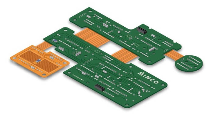
Hybrid Material Stackups: A Cost-Effective Compromise
Because low-loss materials are significantly more expensive than FR-4, it is often uneconomical to build an entire high-layer-count board out of them, especially if only a few of the layers carry critical high-speed signals. A common and cost-effective solution is to use a hybrid stackup. In this approach, designers strategically place layers of expensive, ultra-low-loss material where the fastest signals will be routed, while using less expensive, mid-loss or even FR-4-like materials for power planes, ground planes, and slower signal layers. This requires careful collaboration with the PCB fabricator, as bonding different material types together presents manufacturing challenges, but it provides a powerful method for optimizing both performance and budget.
Advanced Manufacturing & Design Techniques for High-Speed Success
The theoretical design of a high-speed PCB can only be realized through advanced fabrication and assembly techniques. The physical geometries required for high performance are pushing the limits of what is manufacturable.
High-Density Interconnect (HDI) and Miniaturization
High-Density Interconnect (HDI) technology is a set of PCB manufacturing techniques that allow for significantly more components and connections to be packed into a smaller area. This is essential for modern data center line cards and 5G radio units where space is at a premium. HDI utilizes features like microvias (vias with a diameter typically less than 150 microns), which can be laser-drilled, and thinner traces and spaces. This allows for routing out of fine-pitch BGA packages that would be impossible with conventional drilling and routing rules, enabling the use of more powerful and complex chips.
Precision in Practice: Back-Drilling, Vias, and Surface Finishes
Even small physical features on a PCB can become major signal integrity problems at high frequencies. A via that passes through a board to connect two layers leaves an unused portion, or stub, on the other side. At multi-gigabit speeds, this stub acts as an antenna, causing severe signal reflections. To solve this, a process called back-drilling or controlled-depth drilling is used. After the main drilling and plating process, a slightly larger drill bit is used to re-drill the via from the outside-in, removing the unused stub and dramatically improving signal integrity.
The choice of surface finish—the metal coating applied to the copper pads for solderability and protection—also becomes critical. Traditional finishes like Hot Air Solder Leveling (HASL) create an uneven surface that is unsuitable for fine-pitch components. For high-speed boards, smoother and more planar finishes like Electroless Nickel Immersion Gold (ENIG) or Immersion Silver (ImAg) are required to ensure good solder connections and to minimize the “skin effect,” where high-frequency currents travel only on the outer surface of the conductor, making the surface roughness a factor in overall signal loss.
The Future is Faster: What’s Next for High-Speed PCBs?
The demand for speed is relentless. As the industry moves towards 224 Gbps data rates and explores 6G technologies in the Terahertz (THz) range, the challenges for PCBs will only intensify. The future will likely see even greater integration of technologies directly onto or into the PCB. This includes the co-packaging of optics and electronics (CPO), where optical engines are placed on the same substrate as the switch ASIC to drastically shorten electrical path lengths. We will also see more advanced materials, possibly with even lower Dk/Df values or integrated functionalities. Furthermore, the role of Artificial Intelligence (AI) and Machine Learning (ML) in PCB design will grow, helping engineers to optimize the incredibly complex routing and layout of next-generation boards in ways that are beyond human capability alone.
Conclusion: The Silent Enabler of Our Connected World
High-speed PCBs are far more than simple green boards with copper lines; they are sophisticated, highly engineered systems that form the physical layer of our digital infrastructure. From the 5G towers connecting our cities to the hyperscale data centers powering the cloud, their performance is paramount. Success in this domain requires a holistic approach, mastering the intricate dance between signal integrity, power delivery, and thermal management. By leveraging revolutionary low-loss materials and pushing the boundaries of manufacturing precision, PCB designers and engineers are the silent enablers, building the robust and reliable foundation upon which the future of high-speed communication rests.