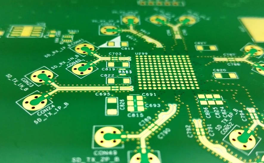
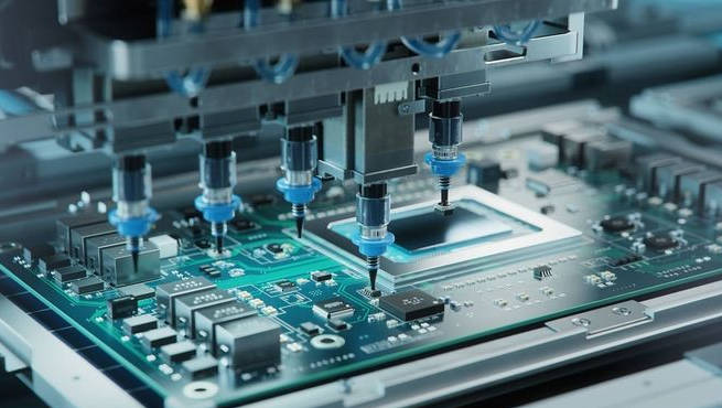
In the world of high-speed electronics, the difference between a successful design and a costly failure often hinges on a single, critical principle: impedance matching. For engineers and designers working with High-Frequency PCB technology, a cursory understanding is insufficient. This guide provides a deep dive into the theory, practical application, and manufacturing considerations for achieving optimal signal integrity.

Part I: The Imperative of Impedance Matching
Impedance matching is the synchronization of impedance across a signal path. Unlike simple DC resistance, impedance is a dynamic property that a high-frequency signal encounters as it travels along a transmission line. When the impedance of the source, the transmission line, and the load are unequal, signal energy is reflected back toward the source.
The ramifications of this mismatch are profound and multifaceted:
- Signal Integrity Degradation: Reflections cause a multitude of signal integrity issues, including ringing, overshoot, undershoot, and jitter, which can push a signal outside the receiver’s voltage thresholds, leading to Bit Error Rate (BER) increases. On a Time Domain Reflectometer (TDR) plot, these issues appear as deviations from the target impedance line.
- Radiated Emissions (EMI): Signal reflections create standing waves on the PCB trace, which act as highly efficient antennas. This can cause the board to radiate electromagnetic energy, potentially failing strict EMI/EMC compliance standards. A reputable high frequency pcb manufacturer will understand how their fabrication process can impact these emissions.
- Power Transfer Inefficiency: In RF and microwave circuits, maximum power transfer is only possible when impedances are matched. A mismatch results in significant power loss, measured by the Return Loss (S11) parameter, which is a critical metric for any high frequency pcb design.
Part II: Deep Dive into Characteristic Impedance (Z0)
The characteristic impedance of a trace is determined by a precise interplay of geometric and material properties. The formula for characteristic impedance, though complex, highlights the key variables:
Where L is the inductance per unit length and C is the capacitance per unit length of the trace.
Factors Influencing Z0
- Dielectric Material (ϵr): The dielectric constant of the PCB material is a major factor. A lower ϵr results in a higher impedance, and a higher ϵr results in a lower impedance. Standard FR-4 has an ϵr that can vary with frequency, making it less ideal for precision high-frequency work. Specialized materials from high frequency pcb supplier companies like Rogers or Isola offer stable, low ϵr and a low dissipation factor (tanδ) to minimize signal loss.
- Stack-up Geometry: The physical layout of the layers is paramount.
- Trace Width (W): A wider trace lowers impedance.
- Trace Thickness (T): A thicker trace lowers impedance.
- Height to Reference Plane (H): A greater distance to the reference plane increases impedance.
The precise calculations for these values are complex and are best handled by dedicated field solvers in modern PCB design software.
Part III: Advanced Design & Manufacturing Techniques
Achieving controlled impedance requires careful planning from the initial high frequency pcb design phase.
Common Transmission Line Structures
| Topology | Description | Advantages & Applications |
| Microstrip Line | A trace on the outer layer separated from a ground plane by the core/prepreg material. | Simple and cost-effective. Suitable for designs up to a few GHz. Requires careful placement to minimize external interference. |
| Stripline | A trace embedded between two ground planes. | Provides excellent EMI shielding and isolation. The impedance is less sensitive to layer-to-layer variations. Ideal for high-density, multi-layer designs where internal signal layers are used. |
| Coplanar Waveguide | A trace on a layer with ground fills on either side and a ground plane beneath. | Offers superior signal isolation and is excellent for RF applications. The impedance is highly controllable and less susceptible to the effects of adjacent traces. |
Mitigating Impedance Discontinuities
1.Vias: Vias represent a significant impedance discontinuity. As the signal travels through a via, it encounters a change in its environment, causing reflections. For extremely high-frequency designs (e.g., beyond 10 Gbps), a technique called back-drilling is used. A high frequency pcb manufacturer uses a second drill pass to remove the unused, non-functional portion of a via barrel, eliminating the stub and its associated reflections.
2.Routing Corners: Any abrupt change in trace direction is a discontinuity. While a 90-degree bend is acceptable at low frequencies, it is a significant source of reflection at high speeds. Use 45-degree bends or, for critical traces, smooth arcs to maintain a consistent impedance path.
3.Differential Pair Routing: For high-speed differential signals, maintaining strict length and spacing matching is critical to avoid mode conversion and common-mode noise. A typical tolerance is 5 mils or less over the entire length.
Part IV: Verification and Quality Control
The final and most crucial step is to verify the impedance after high frequency pcb manufacturing. A reputable high frequency pcb supplier will perform these tests as part of their quality assurance process.
Key Measurement Tools
- Time Domain Reflectometer (TDR): This is the definitive tool for measuring impedance. It sends a fast rise-time pulse down a trace and measures the reflection profile. A TDR can precisely locate impedance discontinuities (e.g., vias, connectors, abrupt width changes) and measure their magnitude.
- Vector Network Analyzer (VNA): Used primarily for RF circuits, a VNA measures the S-parameters of a circuit, providing a frequency-domain view of performance. It is used to measure Return Loss (S11), which directly quantifies how much signal is reflected.
Conclusion: A Holistic Approach to High-Frequency Design
Impedance matching is not an isolated task but an integrated part of the entire high frequency pcb design and manufacturing process. It requires informed decisions on materials, a deep understanding of layout techniques, and close collaboration with your high frequency pcb manufacturer. By adopting a comprehensive, detail-oriented approach, you can ensure the signal integrity and reliability of your high-frequency products, from the drawing board to the final product.


