While traditional PCB manufacturing remains the backbone of mass-produced electronics, 3D printed PCBs are rapidly emerging as a disruptive force, particularly for rapid prototyping, complex designs, and customized applications. The future of circuit board fabrication is unlikely to see one method dominate the other; instead, we will witness a symbiotic coexistence where each technology excels in its designated role, creating a more agile and innovative electronics industry.
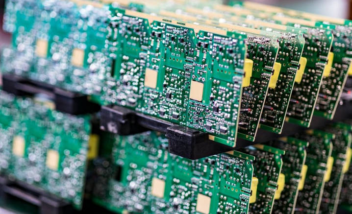
Table of Contents
- Understanding the Incumbent: Traditional PCB Manufacturing
- The Challenger Emerges: 3D Printed PCBs
- A Head-to-Head Showdown: 3D Printed vs. Traditional PCBs
- Application Deep Dive: Choosing the Right Technology for the Job
- The Future of Circuit Board Fabrication: Coexistence, Not Conquest
- Final Verdict: A Symbiotic Future
Understanding the Incumbent: Traditional PCB Manufacturing
For decades, traditional Printed Circuit Board (PCB) manufacturing has been the undisputed standard for creating the electronic nervous systems of our devices. This highly refined process, known as subtractive manufacturing, is responsible for virtually every mass-produced electronic gadget in existence, from smartphones to industrial control systems. It is a method built on precision, reliability, and economies of scale, forming the bedrock of the modern electronics supply chain.
How Does Subtractive Manufacturing Work?
The term “subtractive” perfectly describes the core principle of this method: you start with more and remove material to achieve the final design. The process begins with a laminated board, typically made of fiberglass (FR-4), which is fully coated with a layer of conductive copper. The goal is to etch away the unwanted copper, leaving behind only the desired conductive traces, pads, and connections that form the circuit.
This is a multi-step chemical and mechanical procedure. First, a light-sensitive film called a photoresist is applied to the copper surface. A “photomask,” which is a template of the circuit design, is placed over the board, and it’s exposed to UV light. The light hardens the photoresist in the areas that will become the final circuit. The board is then submerged in a chemical developer that washes away the unhardened photoresist, exposing the unwanted copper. Finally, an etchant solution (like ferric chloride) dissolves the exposed copper, leaving the protected circuit traces intact. Subsequent steps involve drilling holes (vias) for multi-layer connections, applying a protective solder mask, and screen-printing component labels (silkscreen).
The Unmistakable Advantages of Traditional Methods
The dominance of traditional PCB manufacturing is rooted in several key strengths. First and foremost is cost-effectiveness at scale. The setup costs for tooling and photomasks are significant, but once production begins, the per-unit cost plummets, making it incredibly efficient for runs of thousands or millions of boards. Secondly, the technology is mature and highly reliable. Decades of refinement have led to standardized processes, predictable results, and exceptional electrical performance, including high conductivity and the ability to handle significant power loads. Material diversity is another major advantage, with a wide range of substrates and finishes available to meet specific performance requirements like high frequency or extreme temperatures.
Where Do Traditional PCBs Fall Short?
Despite its strengths, the subtractive method has notable drawbacks, particularly in the context of modern, fast-paced product development. The primary limitation is speed, especially for prototyping. The lead time for a small batch of prototype boards can range from several days to multiple weeks, creating a significant bottleneck in the design-iterate-test cycle. This process is also inherently wasteful; it involves harsh chemicals and results in significant copper and etchant waste, posing environmental concerns. Furthermore, traditional manufacturing is largely confined to 2D, planar structures. Creating complex, three-dimensional circuits is exceptionally difficult and expensive, limiting design freedom for integrated and non-planar electronics.
The Challenger Emerges: 3D Printed PCBs
In stark contrast to the established subtractive method, 3D printing of PCBs, a form of additive manufacturing, is revolutionizing how we think about circuit fabrication. Instead of starting with a full sheet of copper and etching it away, this technology builds the circuit from the ground up, layer by layer. It deposits conductive and insulating materials precisely where they are needed, opening a new frontier of design possibilities and dramatically accelerating the prototyping process.
What is Additive Manufacturing for Electronics?
Additive manufacturing for electronics involves using specialized printers that can dispense multiple materials. The process typically starts with a digital CAD file of the circuit design. The printer then begins to build the board. A common technique is inkjet printing, where a print head deposits droplets of a non-conductive polymer (the substrate) and a conductive ink (often containing silver nanoparticles) in a precise pattern. The board is built up layer by layer, with the printer seamlessly creating the substrate and embedding the conductive traces within it. This allows for the creation of complex, multi-layer boards without the need for drilling, pressing, and lamination. Other methods include aerosol jet printing for finer features and fused deposition modeling (FDM) with conductive filaments.
The Revolutionary Benefits of 3D Printing Circuits
The most celebrated advantage of 3D printed PCBs is unparalleled speed for prototyping. An engineer can design a circuit in the morning and have a functional, physical prototype in their hands by the afternoon. This ability to produce boards “on-demand” and in-house collapses development cycles from weeks to hours, fostering rapid innovation and iteration. Another transformative benefit is design freedom. Additive manufacturing can easily create non-planar, 3D circuits that conform to the shape of a product, integrating electronics directly into casings, wearables, or sensor housings. This process is also significantly more environmentally friendly, as it only uses the material required for the final product, virtually eliminating the chemical and material waste associated with etching.
Current Limitations and Hurdles for 3D Printed PCBs
While the potential is immense, 3D printed electronics currently face several significant hurdles. The primary limitation is scale and cost for mass production. The per-unit cost of a 3D printed board remains relatively constant, making it far more expensive than traditional methods for large volumes. The electrical performance and durability can also be a concern. The conductivity of printed silver inks is generally lower than that of solid copper, which can be a problem for high-power or high-frequency applications. Furthermore, the resolution (minimum trace width and spacing) of most accessible 3D printers is still lower than what traditional photolithography can achieve, limiting their use for extremely dense, high-performance designs. The technology and materials are still evolving, and standardization is not yet on par with the mature traditional ecosystem.
A Head-to-Head Showdown: 3D Printed vs. Traditional PCBs
To make an informed decision, it’s crucial to understand how these two technologies stack up across key metrics. The “best” choice is not universal; it is entirely dependent on the specific requirements of your project, from production volume to design complexity.
| Attribute | Traditional PCB Manufacturing (Subtractive) | 3D Printed PCBs (Additive) |
|---|---|---|
| Prototyping Speed | Slow (Days to Weeks) | Extremely Fast (Hours) |
| Cost per Unit (Mass Production) | Very Low | High |
| Design Complexity | Primarily 2D (Planar) | Full 3D, Non-Planar, Conformal |
| Material Waste & Environmental Impact | High (Chemical etchants, copper waste) | Very Low (Additive process) |
| Resolution & Feature Size | Very High (Fine traces & spacing) | Lower (Improving but generally less fine) |
| Electrical Performance | Excellent (Solid copper conductivity) | Good but lower conductivity than copper |
| Supply Chain | Requires external fabrication houses | Enables in-house, on-demand production |
Application Deep Dive: Choosing the Right Technology for the Job
The theoretical comparison is clear, but how does it translate into practical decision-making? The choice between traditional and 3D printed PCBs boils down to understanding the specific context and goals of your project. Each technology serves a distinct purpose and excels in different scenarios.
When to Stick with Traditional Manufacturing
Traditional PCB fabrication remains the undisputed king for several key applications. The most obvious is mass production. If you plan to manufacture hundreds, thousands, or millions of a single board design, the economies of scale offered by subtractive manufacturing are unbeatable. The high initial setup cost is amortized over the large volume, resulting in a per-unit price that 3D printing cannot currently match.
You should also opt for traditional methods for high-performance applications. Projects that require very fine trace widths and spacing, such as in modern microprocessors or high-density memory modules, are better served by the superior resolution of photolithography. Similarly, for high-power or high-frequency circuits, the excellent conductivity and signal integrity of solid copper traces on well-characterized dielectric materials are essential for reliable performance.
When to Embrace 3D Printing
3D printing shines brightest in the realm of rapid prototyping and R&D. For engineers and startups needing to quickly test and validate a circuit design, the ability to print a functional board in a few hours is a game-changer. It accelerates innovation by allowing for multiple design iterations in a single day, a process that would take weeks with a traditional fab house. This also protects intellectual property by keeping early-stage designs in-house.
Another powerful use case is for custom, one-off, or low-volume production, such as in specialized medical devices, research equipment, or bespoke industrial machinery. In these scenarios, the high setup cost of traditional manufacturing is prohibitive. 3D printing offers a cost-effective way to produce a small number of highly customized boards. Finally, any project requiring 3D or conformal electronics is a perfect candidate for additive manufacturing. This includes wearable technology where circuits must curve around a wrist, IoT sensors integrated into a product’s housing, or antennas with complex three-dimensional geometries for optimized performance.
The Future of Circuit Board Fabrication: Coexistence, Not Conquest
The question of “which will dominate?” frames the discussion as a zero-sum game. However, the future of electronics manufacturing is far more likely to be a collaborative one. These technologies are not just competitors; they are complementary tools in a growing toolkit. The real innovation will come from leveraging the strengths of each, and in some cases, combining them.
The Hybrid Model: The Best of Both Worlds?
An exciting prospect is the rise of a hybrid manufacturing model. Imagine using 3D printing to create a complex, multi-layer board with embedded components and unique 3D structures. This board could then be finished using traditional processes to add a final layer of high-density traces or a specific surface finish for robust component soldering. Another hybrid approach involves using 3D printing to create custom fixtures, stencils, or even test jigs that support and streamline the traditional manufacturing workflow. This synergy allows designers to harness the speed and complexity of 3D printing while still benefiting from the reliability and performance of established methods.
What Innovations Will Shape the Future?
The trajectory of 3D printed electronics will be defined by advancements in several key areas. Material science is at the forefront. The development of new conductive inks with conductivity closer to that of copper, as well as a wider array of robust, high-performance dielectric polymers, will be crucial for expanding the range of applications. Additionally, progress in multi-material printers that can seamlessly combine rigid substrates, flexible materials, conductive traces, and even passive components like resistors and capacitors in a single print job will unlock unprecedented levels of integration. As printer resolution improves and costs decrease, the line between prototyping and small-scale production will continue to blur.
Final Verdict: A Symbiotic Future
So, which technology will dominate? The answer is neither, and both. Traditional PCB manufacturing will continue to be the workhorse for the mass production of the vast majority of our electronics, prized for its cost-efficiency, reliability, and performance at scale. It will not be replaced anytime soon for applications where volume is the primary driver.
At the same time, 3D printed PCBs will become an indispensable tool for innovation, research, and customization. They will dominate the world of rapid prototyping, enabling engineers to create and test at the speed of thought. They will also unlock entirely new product categories through conformal and 3D electronics that were previously impossible to build. The future is not about a single victor, but about a dynamic, symbiotic relationship where designers choose the right tool for the job, leveraging the strengths of both subtractive and additive manufacturing to build the next generation of electronic devices more quickly, creatively, and efficiently than ever before.
3D Printed PCBs, Traditional PCB Manufacturing, Additive Manufacturing, Subtractive Manufacturing, PCB Prototyping, 3D printing electronics, advantages of 3D printed PCBs, how does traditional PCB manufacturing work, future of PCB manufacturing, cost of 3D printed vs traditional PCBs, limitations of 3D printed circuits, Printed Circuit Board, electronics manufacturing, circuit board fabrication, additive vs subtractive

