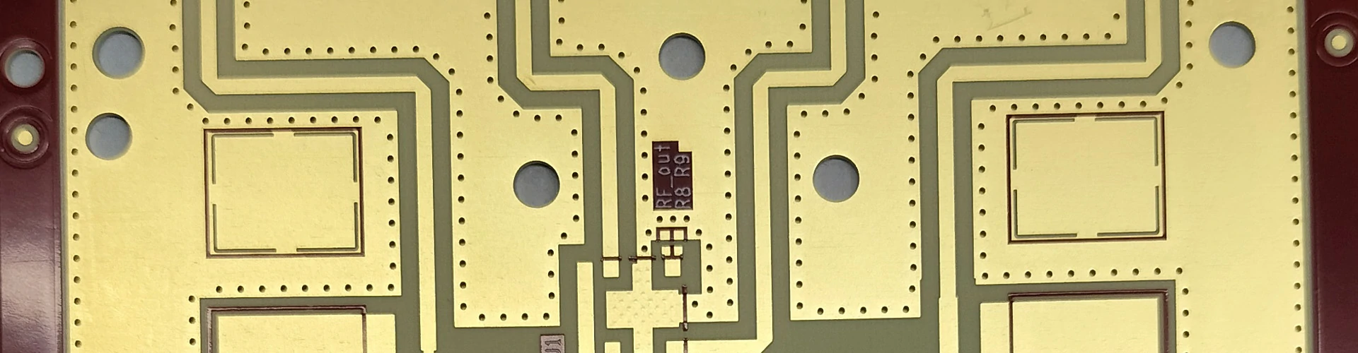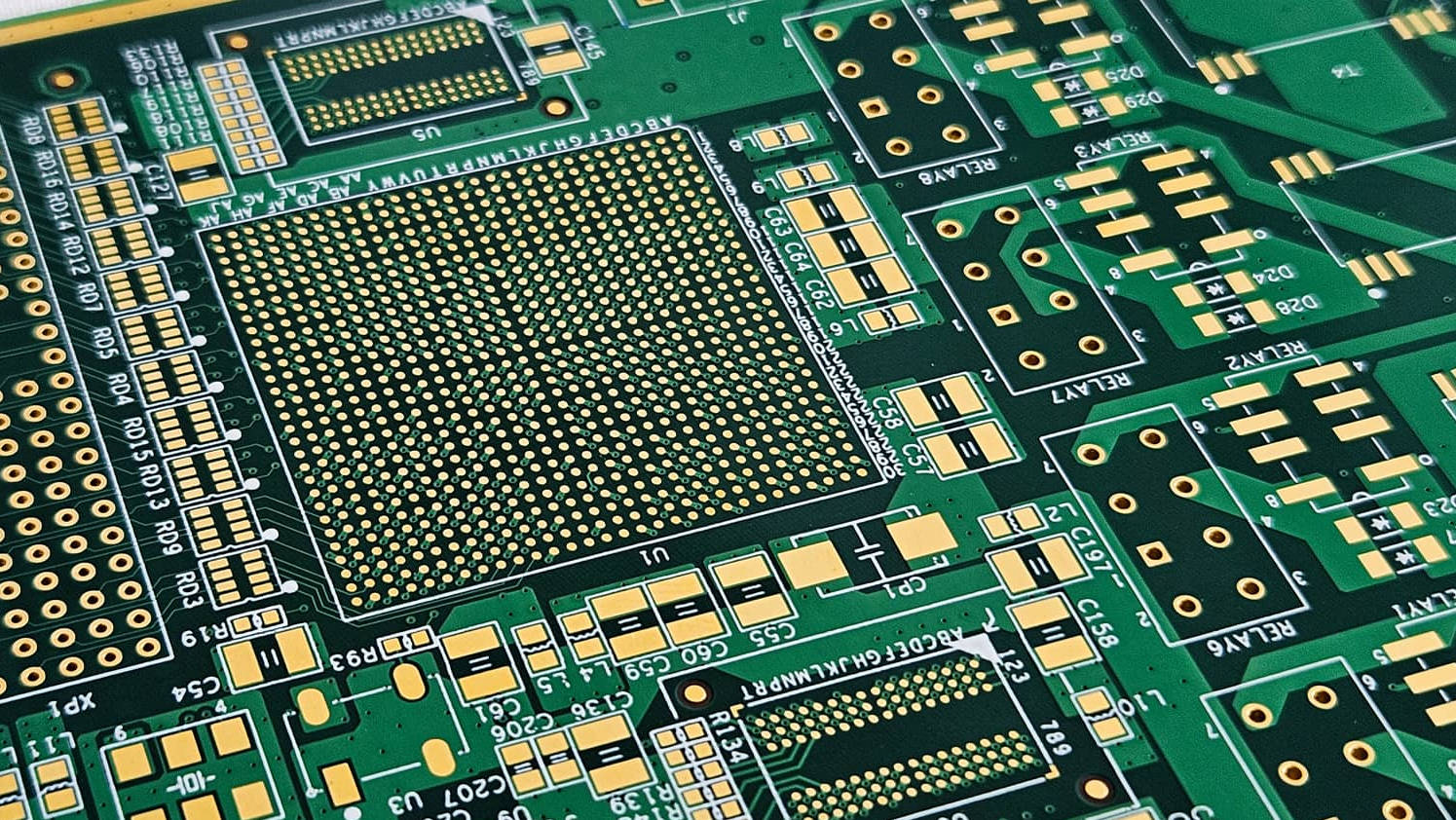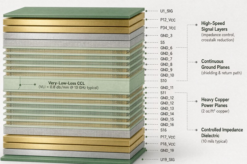
Via-in-pad is usually better for high-speed PCB designs that require dense BGA fanout, shorter signal paths, reduced parasitic effects, and compact HDI routing. Traditional vias are usually better for simpler layouts, lower-cost boards, easier manufacturing, and designs that have enough routing space.
In other words, via-in-pad is not automatically better for every PCB. It is a more advanced structure that can improve routing density and signal integrity when used correctly, but it also increases fabrication complexity and cost. Traditional vias remain practical and reliable for many high-speed PCB projects when routing space, impedance control, and signal path requirements are manageable.
For B2B buyers, the key question is not only “Which via type is better?” A more practical question is: Does your PCB design require the extra density, shorter transition path, and HDI capability that via-in-pad provides?
If your product uses fine-pitch BGA components, high-speed interfaces, dense multilayer routing, or strict signal integrity requirements, you should discuss via structure early with a high-speed PCB manufacturing partner. The final choice affects stackup, impedance, soldering reliability, assembly yield, inspection, cost, and production repeatability.
What Is a Traditional Via in PCB Design?
A traditional via is a plated hole that connects copper layers in a PCB. It is usually placed beside the component pad, not directly inside it. In many layouts, the signal leaves the component pad through a short trace and then enters the via. This structure is often called a “dog-bone” fanout when used with BGA packages.
Traditional vias include through-hole vias, blind vias, buried vias, and microvias, depending on the board layer structure and fabrication method. For many standard multilayer PCBs, traditional through-hole vias are still widely used because they are familiar, cost-effective, and easier to manufacture.
Traditional vias are commonly used for:
| Application | Why Traditional Via Is Used |
|---|---|
| General signal routing | Simple and cost-effective layer transition |
| Power and ground connection | Easy to connect planes across layers |
| Moderate-density PCB layout | Enough space is available for fanout |
| Prototype PCB | Lower fabrication complexity |
| Non-fine-pitch components | No need for advanced HDI structures |
| Cost-sensitive products | Manufacturing is usually more economical |
Traditional vias are not outdated. They remain a practical choice for many high-speed PCBs when the board has enough area, the BGA pitch is not too tight, and the signal transition length does not create serious performance issues.
What Is Via-in-Pad in PCB Design?
Via-in-pad, often called VIP, is a PCB design technique where a via is placed directly inside the surface-mount component pad. This is especially common under fine-pitch BGA pads, where there may not be enough space to route a trace from the pad to a nearby traditional via.
Via-in-pad is widely used in HDI PCB designs, compact electronic products, dense BGA layouts, and high-speed interconnects. Altium describes via-in-pad as placing a plated via directly under a surface-mount pad, commonly for BGA or fine-pitch components, instead of routing traces out to a nearby via.
In many cases, via-in-pad requires the via to be filled and plated over. This helps create a flat solderable surface and prevents solder from flowing into the via during assembly. Altium notes that when BGA pads are placed directly on vias, the vias are filled and plated over to prevent solder ball wicking into the via.
Via-in-pad is commonly used for:
| Application | Why Via-in-Pad Is Used |
|---|---|
| Fine-pitch BGA fanout | Enables routing when dog-bone fanout is not possible |
| High-density PCB | Saves board space |
| HDI PCB | Supports compact multilayer routing |
| High-speed signal transition | Shortens path from pad to internal layer |
| Power delivery under ICs | Can improve dense power/ground connections |
| Compact electronic products | Helps reduce PCB size |
Via-in-pad is most useful when traditional fanout consumes too much space or creates unnecessary signal path length in a dense high-speed PCB.
Via-in-Pad vs Traditional Via: Main Comparison
| Factor | Via-in-Pad | Traditional Via |
|---|---|---|
| Via location | Directly in the component pad | Beside the pad or away from component |
| Routing density | Higher | Lower to moderate |
| BGA fanout capability | Better for fine-pitch BGA | Better for larger-pitch components |
| Signal path length | Shorter | Longer due to dog-bone trace |
| Signal integrity | Can be better when properly designed | Good for many designs, but longer transition may add parasitics |
| Manufacturing complexity | Higher | Lower |
| Cost | Higher | Lower |
| Assembly risk | Requires filled/capped process to avoid solder issues | Easier soldering in many cases |
| Inspection and process control | More demanding | More straightforward |
| Best use case | HDI, fine-pitch BGA, dense high-speed PCB | Standard multilayer PCB, moderate density, cost-sensitive products |
Which Is Better for High-Speed PCB?
For high-speed PCB design, via-in-pad is better when the board needs compact BGA escape routing, shorter signal transitions, reduced parasitic inductance, and dense HDI routing. Traditional vias are better when the layout has enough space and cost control is more important than maximum density.
The right choice depends on several practical questions:
- Is the component package fine-pitch BGA?
- Is there enough room for dog-bone fanout?
- Are the high-speed signals sensitive to via stub and transition length?
- Does the design require HDI stackup?
- Can the PCB supplier support filled and capped via-in-pad reliably?
- Is the project cost-sensitive?
- Will the board move from prototype to volume production?
For example, a dense BGA-based communication board may need via-in-pad because traditional via fanout would consume too much space. On the other hand, an industrial controller with larger components and moderate routing density may use traditional vias successfully without the extra cost of via-in-pad.
Why Via Choice Matters in High-Speed PCB Projects
In high-speed PCB design, vias are not only mechanical holes. They are electrical structures that influence impedance, parasitic capacitance, parasitic inductance, return current path, signal reflection, power integrity, and EMI behavior.
A poorly selected via structure can lead to:
- Impedance discontinuity
- Signal reflection
- Eye diagram degradation
- Increased insertion loss
- Crosstalk around dense routing areas
- Poor BGA escape routing
- Solder joint defects
- Increased rework or redesign cost
Sierra Circuits explains that via-in-pad structures can shorten the signal path and help reduce parasitic effects, which can support signal integrity in dense and high-speed designs.
For purchasing teams, this means via structure is not only a design detail. It affects manufacturability, assembly quality, test strategy, and long-term reliability. If your board uses high-speed ICs or fine-pitch BGA packages, the via decision should be reviewed before fabrication, not after Gerber release.
Signal Integrity: Via-in-Pad vs Traditional Via
Via-in-Pad Signal Integrity Advantages
Via-in-pad can improve signal integrity mainly because it reduces the distance between the component pad and the layer transition. In a traditional dog-bone structure, the signal travels from the pad through a short escape trace and then enters the via. In via-in-pad, the transition happens directly at the pad.
This shorter path can reduce parasitic inductance and capacitance, especially in dense high-speed circuits. PCBSync notes that for high-frequency designs, eliminating the dog-bone trace can improve signal integrity by shortening the signal path and reducing parasitic effects.
Via-in-pad may help in:
| High-Speed Concern | How Via-in-Pad Can Help |
|---|---|
| Long dog-bone fanout | Reduces transition length |
| Dense BGA escape | Enables direct layer transition |
| Impedance discontinuity | Can reduce unnecessary trace/via transition effects |
| Routing congestion | Frees routing channels |
| High-speed differential pairs | Supports compact escape routing |
| Power/ground connection | Can provide direct connection under IC pads |
Traditional Via Signal Integrity Considerations
Traditional vias can still perform well in high-speed PCB designs when properly placed and modeled. The main issue is that they may require longer pad-to-via traces and larger fanout areas. In many applications, this is acceptable. In very dense or very high-speed applications, it may become a limitation.
Traditional vias may be suitable when:
- The BGA pitch is large enough for dog-bone fanout
- Signal speeds are manageable
- The via stub is not excessive
- The board has enough routing space
- Impedance can be controlled within the stackup
- Cost is a major project constraint
Traditional vias are not poor-quality structures; they simply require more routing space and may introduce longer transitions than via-in-pad.
BGA Fanout: Where Via-in-Pad Often Wins
One of the strongest reasons to use via-in-pad is BGA fanout. As BGA pitch becomes smaller, routing traces between pads becomes more difficult. Traditional dog-bone fanout may not leave enough space for trace width, clearance, and manufacturing tolerance.
Via-in-pad allows the designer to route directly from the BGA pad to an internal layer. This saves space and can make dense component placement feasible. Altium states that via-in-pad can help make layouts feasible when space is limited or BGA pitch is shrinking.
| BGA Condition | Recommended Via Strategy |
|---|---|
| Large-pitch BGA with enough routing channels | Traditional via may be sufficient |
| Medium-pitch BGA with moderate density | Traditional via or microvia, depending on layout |
| Fine-pitch BGA with limited escape space | Via-in-pad is often preferred |
| Very dense HDI design | Via-in-pad with microvia may be required |
| High-speed BGA package | Via-in-pad may help reduce transition length |
For dense high-speed boards, via-in-pad is often not just an optimization. It may be necessary to complete the layout.
Manufacturing Process Differences
Traditional Via Manufacturing
Traditional vias are easier to fabricate because they do not usually need to become part of the soldering pad. The via is drilled, plated, and finished according to normal PCB manufacturing processes. Depending on the application, traditional vias may be tented, plugged, filled, or left open.
Traditional vias usually have fewer assembly risks because solder is not placed directly over the via barrel.
Via-in-Pad Manufacturing
Via-in-pad is more demanding. Since the via sits directly inside the solder pad, the surface must be suitable for component placement and soldering. In many BGA applications, this means the via must be filled and capped or plated over.
A common via-in-pad process may include:
| Process Step | Purpose |
|---|---|
| Laser or mechanical drilling | Creates the via hole |
| Copper plating | Connects the required layers |
| Via filling | Prevents voids and solder wicking |
| Planarization | Creates a flat surface |
| Copper capping or plating over | Provides solderable pad surface |
| Surface finish | Supports assembly and corrosion protection |
| Inspection | Confirms reliability and surface quality |
A via-in-pad design should normally be reviewed with the PCB manufacturer because filling, capping, plating, flatness, and assembly reliability depend on process capability.
Cost Comparison: Via-in-Pad vs Traditional Via
Via-in-pad usually costs more than traditional via because it requires more processing steps, tighter quality control, and sometimes HDI manufacturing. The cost difference depends on via type, board layer count, material, hole size, via filling requirement, inspection level, and production volume.
| Cost Factor | Via-in-Pad | Traditional Via |
|---|---|---|
| Drilling complexity | Higher if microvias are used | Lower for standard through vias |
| Filling and capping | Often required | Usually not required |
| Surface flatness control | Critical | Less critical |
| Inspection requirement | Higher | Lower |
| Manufacturing yield sensitivity | Higher | Lower |
| Unit cost | Higher | Lower |
| Redesign cost risk | Lower in dense designs if correctly used | Higher if routing becomes impossible |
For simple PCBs, traditional vias usually offer better cost efficiency. For dense high-speed PCBs, via-in-pad may reduce total project risk because it enables compact routing, improves fanout feasibility, and may avoid a larger board or additional layout iterations.
Reliability and Assembly Considerations
Via-in-pad can improve routing density, but incorrect implementation can cause assembly defects. The main risk is solder wicking. If the via is open or poorly filled, solder may flow into the via during reflow, reducing solder volume under the component pad and causing weak joints, voids, or unreliable connections.
For BGA pads, filled and capped via-in-pad is often preferred because it creates a flatter and more reliable soldering surface. NextPCB notes that filling and capping help create flatness for fine-pitch components and avoid surface defects that could affect assembly.
Traditional vias are generally easier from an assembly perspective because they are not directly under the solder joint. However, if traditional vias are placed too close to pads without proper solder mask control, solder bridging or solder loss can still occur.
Engineering Selection Guide
Use the following table as a practical decision guide.
| Design Requirement | Better Choice | Reason |
|---|---|---|
| Fine-pitch BGA escape routing | Via-in-pad | Saves space and enables dense fanout |
| Cost-sensitive standard PCB | Traditional via | Lower fabrication complexity |
| Short high-speed signal path | Via-in-pad | Reduces dog-bone transition length |
| Simple industrial control board | Traditional via | Usually sufficient and economical |
| Compact HDI product | Via-in-pad | Supports high-density routing |
| Easy prototype manufacturing | Traditional via | Faster and simpler fabrication |
| High-speed differential pair under BGA | Via-in-pad may be preferred | Helps compact escape routing |
| Larger board with enough routing space | Traditional via | Cost-effective and reliable |
| Strict assembly flatness under BGA | Filled/capped via-in-pad | Reduces soldering risk |
| Lower layer-count design | Traditional via | Avoids unnecessary HDI cost |
Common Mistakes When Choosing Via-in-Pad or Traditional Via
Mistake 1: Using Via-in-Pad Without Filling or Capping
Open vias inside solder pads can cause solder wicking and assembly defects. Via-in-pad under BGA pads should be specified clearly in the fabrication notes.
Mistake 2: Choosing Traditional Via for Fine-Pitch BGA Without Checking Escape Routing
Some teams discover too late that dog-bone fanout is impossible with their BGA pitch and manufacturing rules. This can force a redesign.
Mistake 3: Treating Via Choice as Only a Layout Decision
Via choice affects fabrication, assembly, impedance, inspection, and cost. It should involve both the design team and PCB manufacturer.
Mistake 4: Ignoring Via Stub Effects
In high-speed PCB design, via stubs can create signal integrity problems. Depending on signal speed, stackup, and via depth, back drilling, blind vias, microvias, or via-in-pad may be considered.
Mistake 5: Sending Files Without Clear Via Requirements
If your design includes via-in-pad, clearly specify which vias need filling, capping, plating over, or special inspection. Do not assume the manufacturer will interpret all via structures correctly without notes.
How to Work With a High-Speed PCB Supplier
When your design includes via-in-pad, traditional vias, HDI structures, or controlled impedance, supplier communication is critical. You should provide more than basic Gerber files.
Prepare the following information:
| Information to Provide | Why It Matters |
|---|---|
| Layer stackup | Defines via depth and reference planes |
| Via type requirements | Clarifies through via, blind via, buried via, microvia, or via-in-pad |
| Filled/capped via notes | Prevents assembly misunderstanding |
| Controlled impedance table | Supports signal integrity |
| Critical net list | Helps review high-speed routes |
| BGA pitch information | Confirms fanout feasibility |
| Material requirement | Affects loss, impedance, and reliability |
| Copper thickness | Affects plating and impedance |
| Assembly requirement | Ensures pad flatness and solderability |
A capable high-speed PCB fabrication service should be able to review via structure, stackup, impedance control, and manufacturing feasibility before production starts.
How to Choose a PCB Manufacturer for Via-in-Pad High-Speed Boards
For via-in-pad high-speed PCB projects, supplier capability is especially important. Not every PCB manufacturer can support filled and capped via-in-pad with stable quality.
When evaluating a supplier, check whether they can support:
- Filled and capped via-in-pad process
- HDI PCB fabrication
- Microvia, blind via, and buried via options
- Controlled impedance manufacturing
- Multilayer stackup review
- BGA fanout manufacturability review
- Surface flatness control for assembly
- Prototype-to-production consistency
- Clear DFM feedback before production
For purchasing managers, price should not be the only factor. A cheaper quotation may become expensive if the supplier cannot produce reliable via-in-pad structures or if assembly defects appear after PCB delivery.
If your design uses dense BGA components or high-speed channels, consider working with a controlled impedance high-speed PCB manufacturer that can support both design review and reliable fabrication.
FAQ
1. Is via-in-pad better than traditional via for high-speed PCB?
Via-in-pad is better when the design needs dense BGA fanout, shorter signal transitions, compact HDI routing, or reduced parasitic effects. Traditional via is better for simpler boards, lower cost, and layouts with enough routing space.
2. When should I use via-in-pad in PCB design?
You should consider via-in-pad when using fine-pitch BGA packages, dense multilayer routing, high-speed signal escape, compact board size, or HDI PCB structures where traditional dog-bone fanout is not practical.
3. Does via-in-pad improve signal integrity?
Via-in-pad can improve signal integrity by shortening the transition between the component pad and internal routing layer. This may reduce parasitic inductance and capacitance, especially in dense high-speed PCB designs.
4. Why does via-in-pad need to be filled and capped?
Via-in-pad often needs filling and capping to create a flat solderable pad and prevent solder from flowing into the via during reflow. This is especially important for BGA assembly reliability.
5. Is traditional via still suitable for high-speed PCB?
Yes. Traditional vias are still suitable for many high-speed PCBs when routing space is available, via stubs are controlled, impedance is managed, and the design does not require fine-pitch BGA fanout.
6. Is via-in-pad more expensive than traditional via?
Yes, via-in-pad is usually more expensive because it often requires filling, planarization, capping, tighter inspection, and more advanced fabrication control. However, it may reduce total project risk in dense HDI designs.
7. What should I tell my PCB manufacturer if I use via-in-pad?
You should provide via filling and capping requirements, stackup, impedance targets, BGA pitch, critical nets, material requirements, and assembly expectations. Clear documentation helps prevent soldering and manufacturing issues.
Conclusion
Via-in-pad and traditional via both have important roles in high-speed PCB design. Via-in-pad is usually the better choice for fine-pitch BGA fanout, HDI routing, compact layouts, and short high-speed transitions. Traditional via remains a practical and cost-effective option for standard multilayer boards, moderate-density layouts, and designs with enough routing space.
The best via choice depends on signal speed, BGA pitch, routing density, impedance requirements, assembly reliability, and manufacturing capability.
For B2B high-speed PCB projects, via selection should be reviewed early with the PCB manufacturer. If your board includes dense BGA packages, controlled impedance signals, or HDI routing, a professional high-speed PCB supplier can help evaluate whether via-in-pad, traditional via, microvia, blind via, or a mixed via strategy is more suitable for your design.