I. Introduction: The Critical Interface of IC Packaging
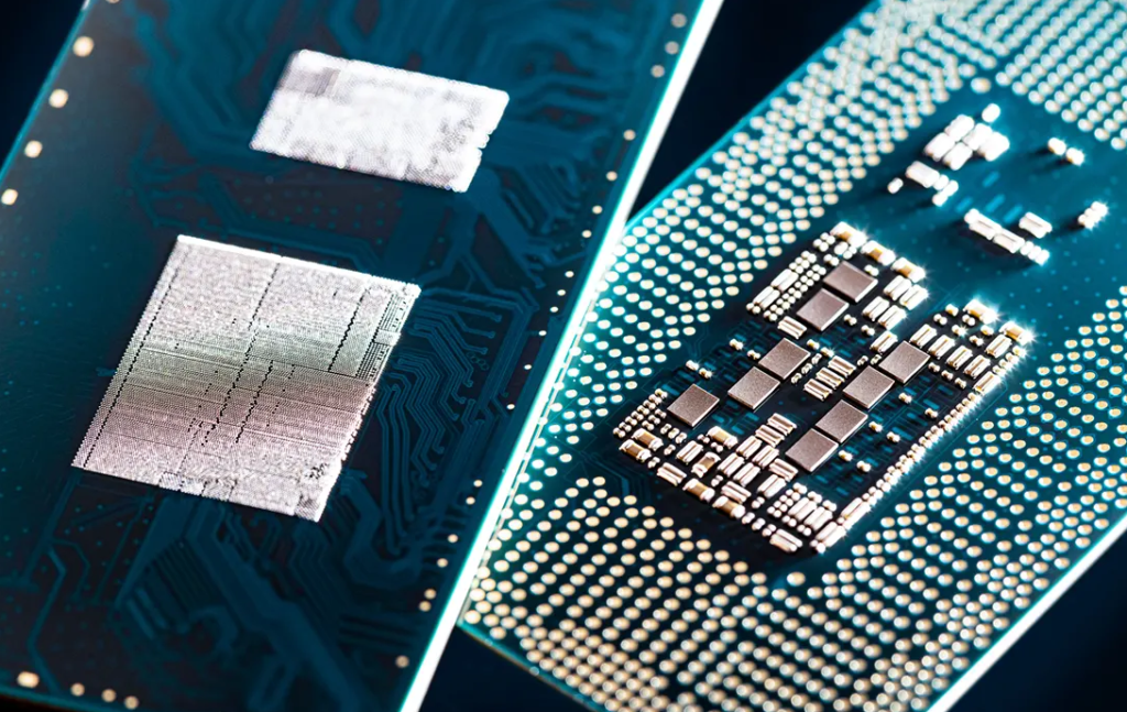
In the intricate world of microelectronics, the integrated circuit (IC) die is the brain, but it’s the IC package that acts as its vital interface to the outside world. Without proper packaging, a delicate semiconductor die, often no larger than a fingernail, would be vulnerable to physical damage, unable to connect to a printed circuit board (PCB), and incapable of dissipating the heat it generates. IC packaging is far more than just a protective shell; it’s a sophisticated engineering discipline that enables electrical connectivity, manages thermal dissipation, provides mechanical protection, and defines the final form factor of the electronic component.
For anyone involved in IC substrate manufacturing, understanding the different types of IC packages isn’t just beneficial—it’s absolutely crucial. The specific requirements of an IC package directly dictate the design, materials, and complex IC substrate manufacturing process. From the number of layers and line widths to the types of vias and thermal management features, every aspect of the substrate is tailored to the demands of the package it will support.
The evolution of IC packages mirrors the relentless drive for miniaturization and enhanced performance in electronics. From the early, bulky Dual In-line Packages (DIPs) to today’s incredibly dense array packages, the industry has continuously innovated to pack more transistors into smaller spaces, demanding ever more advanced IC substrate technologies.
II. Fundamentals of IC Packaging: Key Considerations for Substrate Design
Before diving into specific package types, it’s essential to grasp the fundamental components and the critical factors that influence package selection.
A. Basic Components of an IC Package
Every IC package, regardless of its type, typically comprises several core elements:
- Semiconductor Die (Chip): The silicon chip where the integrated circuit’s functionality resides.
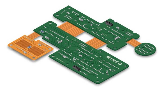
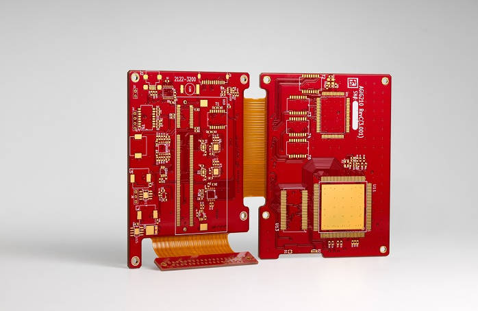
- Lead Frame / Substrate: This is the base upon which the die is mounted. In modern, high-density packages, this is primarily an IC substrate – a multi-layered PCB-like structure specifically designed for IC mounting, with fine lines and microvias.
- Bonding Wires / Solder Bumps: These are the electrical connections between the IC die and the lead frame or substrate. Wire bonding uses fine gold or copper wires, while flip-chip technology uses tiny solder bumps directly connecting the die to the substrate.
- Encapsulant (Molding Compound): A plastic or epoxy material that encapsulates and protects the die and its interconnections from environmental factors like moisture, dust, and physical shock.
- Heat Spreader / Heat Sink: Components, often made of copper or aluminum, designed to efficiently dissipate heat generated by the IC, particularly in high-power applications.
B. Key Factors Influencing Package Type Selection
The choice of an IC package type is a multi-faceted decision driven by a complex interplay of design requirements and constraints. IC substrate manufacturers must be acutely aware of these factors, as they directly impact the design and fabrication of the substrate:
| Factor | Description | Impact on IC Substrate Manufacturing |
| Electrical Performance | Signal integrity, impedance matching, power delivery, parasitic inductance/capacitance. | Demands low Dk/Df materials, controlled impedance traces, effective power planes. |
| Thermal Management | Efficiency of heat dissipation to prevent overheating and ensure reliability. | Requires thermal vias, embedded copper planes, specific material CTEs, and sometimes integrated heat sinks. |
| Mechanical Protection | Robustness against physical shock, vibration, and environmental exposure. | Influences substrate thickness, material rigidity, and overall package stacking. |
| Form Factor & Size | Overall footprint, height, and shape constraints for the end product. | Drives miniaturization; requires finer lines, smaller vias, and potentially thinner substrates. |
| Pin Count & I/O Density | Number of external connections and how densely they are packed. | Determines the number of layers, microvia density, and pad pitch on the substrate. |
| Cost | Manufacturing complexity, material expenses, testing. | Balancing advanced features (e.g., more layers, finer lines) with cost-effective processes. |
| Assembly Method | Compatibility with Through-Hole Technology (THT) or Surface Mount Technology (SMT). | Dictates pad design (THP vs. SMD pads), solder mask features, and overall substrate layout. |
| Reliability | Expected operational lifetime, resistance to temperature cycles, humidity. | Influences material selection (e.g., low CTE for thermal cycling), process control for defect prevention. |
III. Classification of IC Packages: A Comprehensive Overview
IC packages can be broadly categorized based on their method of mounting onto a PCB: Through-Hole Technology (THT) or Surface Mount Technology (SMT). Within SMT, array packages represent the cutting edge for high-density applications.
A. Through-Hole Technology (THT) Packages (Briefly)
These are older package types designed to have leads inserted into drilled holes on a PCB and then soldered. While less common in new designs, they still have niche applications.
- 1. DIP (Dual In-line Package):
- Description: Rectangular package with two rows of leads extending perpendicularly from the body.
- Relevance to substrate: From an IC substrate manufacturing perspective, these require much simpler, less dense substrates with larger pitch through-holes. They are largely obsolete for complex ICs.
B. Surface Mount Technology (SMT) Packages
SMT packages are mounted directly onto the surface of the PCB, allowing for higher component density and automated assembly.
- 1. Small Outline Packages (SOP/SOIC):
- Description: Rectangular packages with “gull-wing” shaped leads extending from two sides. Variants include Small Outline IC (SOIC), Thin Small Outline Package (TSOP), and Shrink Small Outline Package (SSOP).
- Applications: Widely used for memory chips, operational amplifiers, and general-purpose logic ICs.
- Relevance to substrate: These packages require substrates with moderate routing density and standard surface mount pads. IC substrate manufacturers typically handle these with established processes.
- 2. Quad Flat Packages (QFP/LQFP/TQFP):
- Description: Square packages with “gull-wing” leads extending from all four sides. Variants include Low Profile QFP (LQFP) and Thin QFP (TQFP), offering reduced height.
- Applications: Common for microcontrollers, ASICs, FPGAs, and interface chips due to their higher pin counts compared to SOPs.
- Relevance to substrate: QFPs demand higher routing density and finer pitch leads, pushing IC substrate manufacturing towards more precise etching and plating capabilities.
- 3. Leadless Packages (QFN/DFN):
- Description: Quad Flat No-leads (QFN) and Dual Flat No-leads (DFN) are compact packages with no leads extending from the body. Instead, electrical connections are made via pads on the bottom perimeter, often with an exposed thermal pad in the center for improved heat dissipation.
- Applications: Ideal for space-constrained applications like smartphones, wearables, RF modules, and power management ICs.
- Relevance to substrate: These packages place higher demands on the IC substrate, requiring very flat pads, precise solder mask definitions, and often incorporating advanced thermal vias directly beneath the exposed pad for efficient heat transfer.
C. Array Packages (High-Density Interconnect)
These represent a significant leap in packaging technology, enabling extremely high I/O counts by utilizing the entire bottom surface of the package for connections.
- 1. Ball Grid Array (BGA):
- Description: Instead of perimeter leads, BGAs use an array of solder balls on the underside of the package for electrical connection to the PCB. This allows for significantly higher I/O density than QFPs.
- Variations:
- PBGA (Plastic BGA): Uses organic laminate substrate, widely adopted.
- CBGA (Ceramic BGA): Uses ceramic substrate, offering better thermal and electrical performance, but higher cost.
- FCBGA (Flip-Chip BGA): The die is “flipped” and mounted directly onto the substrate using solder bumps, eliminating wire bonds for superior performance.
- Applications: The dominant package for high-performance processors (CPUs, GPUs), FPGAs, chipsets, and high-end ASICs.
- Relevance to IC substrate manufacturing: BGAs are a primary driver for advanced IC substrate manufacturing. They demand multi-layer substrates (often 4 to 16+ layers), microvias (laser-drilled, stacked, and staggered), fine line and space technology (down to 15 µm or less), controlled impedance routing, and the use of advanced low-Dk/Df materials for high-speed signals. IC substrate manufacturers specializing in these packages are at the forefront of the industry.
- 2. Chip Scale Package (CSP):
- Description: A package where the size is no more than 1.2 times the area of the semiconductor die itself. CSPs offer maximum miniaturization.
- Variations:
- Wafer-Level CSP (WLCSP): The package is created directly on the wafer before dicing, offering ultimate compactness.
- Wire-Bond CSP: Uses wire bonds from the die to a small substrate within the package.
- Flip-Chip CSP: Utilizes flip-chip technology for direct die-to-substrate connection.
- Applications: Absolutely critical for space-constrained mobile devices (smartphones, wearables), memory modules (DRAM, Flash), and solid-state drives.
- Relevance to substrate: CSPs require extremely compact and highly integrated IC substrates, often pushing the boundaries of ultra-fine pitch interconnects and advanced build-up layer processes.
- 3. Flip-Chip (FC) Packages:
- Description: In a flip-chip package, the IC die is mounted face-down directly onto the IC substrate using an array of solder bumps (or copper pillars with solder caps). This eliminates the need for bonding wires. An underfill material is typically dispensed between the die and the substrate for mechanical reinforcement and thermal transfer.
- Advantages: Offers superior electrical performance (shorter electrical paths, reduced parasitic inductance), better thermal dissipation (heat flows directly into the substrate), and significantly higher I/O density compared to wire bonding.
- Applications: The preferred packaging method for high-end microprocessors, high-bandwidth memory, network processors, and other high-performance logic devices.
- Relevance to IC substrate manufacturing: Flip-chip packages are arguably the most demanding in terms of IC substrate technology. They require very fine pitch substrate metallization (often necessitating advanced Redistribution Layer (RDL)-like structures on organic substrates), extremely tight planarity control, and materials compatible with the underfill process. Leading IC substrate suppliers must master these complexities.
IV. Advanced Packaging Concepts: Beyond Single Die Packaging
The relentless pursuit of higher integration and performance has led to advanced packaging concepts that go beyond simply enclosing a single IC die. These approaches combine multiple dies or even entire packages within a single assembly.
A. Multi-Chip Modules (MCMs)
- Description: MCMs house multiple semiconductor dies (chips) within a single package, mounted on a common IC substrate. These dies can perform different functions (e.g., CPU, memory, GPU) but are integrated into one component.
- Applications: Used to integrate complex systems in a compact form, common in high-performance computing, networking, and defense applications.
- Relevance to substrate: MCMs require larger, more complex IC substrates that can accommodate multiple die attach areas, extensive inter-die routing, and sophisticated power delivery networks.
B. Package-on-Package (PoP)
- Description: PoP involves stacking multiple standard packages vertically, usually a logic package (e.g., an application processor) on the bottom, with a memory package (e.g., DRAM) stacked on top. The top package connects to the bottom package via solder balls, which in turn connect to the main PCB.
- Applications: Widely adopted in mobile devices (smartphones, tablets) to save space by vertically integrating core logic and memory.
- Relevance to substrate: The bottom package’s IC substrate needs specific design features to facilitate the inter-package connections, including specific pad designs and robust mechanical stability to support the stacked package.
C. 2.5D and 3D Packaging (System-in-Package – SiP)
These concepts represent the forefront of packaging technology, blurring the lines between traditional IC packaging and full system integration. They are often categorized under the umbrella of System-in-Package (SiP).
- 1. 2.5D Packaging:
- Description: Multiple bare dies (e.g., processor, high-bandwidth memory) are placed side-by-side on a silicon interposer. This interposer provides very short, high-bandwidth interconnections between the dies using through-silicon vias (TSVs) or Redistribution Layers (RDLs). The entire interposer-die assembly is then mounted onto a larger IC substrate and encapsulated.
- Advantages: Achieves very high bandwidth and low latency between dies, bypassing traditional PCB routing limitations.
- Relevance to substrate: The IC substrate for 2.5D packages needs to accommodate the relatively large silicon interposer, potentially fine-pitch connections to the interposer, and robust thermal solutions to manage heat from multiple high-power dies. IC substrate manufacturers must ensure excellent flatness and material properties.
- 2. 3D Packaging:
- Description: In true 3D packaging, multiple dies are stacked vertically and interconnected directly using Through-Silicon Vias (TSVs) that pass through the silicon wafers themselves. This creates an extremely compact, high-bandwidth vertical integration.
- Advantages: Achieves extreme miniaturization, ultra-high bandwidth, and reduced power consumption for inter-die communication.
- Relevance to substrate: While much of the direct inter-die connectivity is at the wafer level, the final 3D die stack still needs to be mounted onto an IC substrate for external connectivity to the main PCB. This requires complex, high-performance organic substrates capable of supporting these advanced stacks and managing their thermal outputs.
- D. Embedded Die Packaging:
- Description: This innovative approach involves embedding bare semiconductor dies directly into the layers of an organic IC substrate or even a standard PCB. The die is typically placed in a cavity within the substrate, and subsequent layers are built over it.
- Advantages: Creates an ultra-compact module, significantly reduces parasitic inductance, improves electrical performance, and offers superior thermal management as heat can dissipate directly into the surrounding substrate material. Enhances reliability by protecting the die within the laminate.
- Relevance to IC substrate manufacturing: This is a highly specialized area for IC substrate manufacturers. It requires precision cavity formation, advanced lamination techniques to encapsulate the die without damage, ultra-fine resolution patterning for direct connections to the embedded die, and sophisticated planarization processes to create a flat surface for subsequent layers.
V. Impact on IC Substrate Manufacturing
The diverse landscape of IC package types directly dictates the capabilities and technologies required for IC substrate manufacturing. As packages become more advanced, so too must the substrates.
A. Material Selection
- Low Dk/Df (Dielectric Constant/Dissipation Factor): For high-speed and high-frequency applications (e.g., 5G, AI, HPC), IC substrate suppliers must provide materials with low Dk to minimize signal delay and low Df to reduce signal loss.
- Low CTE (Coefficient of Thermal Expansion): To prevent stress and maintain reliability during temperature cycling, materials with CTE values closely matched to silicon are preferred.
- Enhanced Mechanical Strength: Thinner and more complex substrates require materials that can withstand the manufacturing process and provide long-term reliability.
- Specific Resin Systems and Glass Fabric Types: Different prepreg resins and glass weave patterns affect electrical properties, drillability, and thermal performance, requiring careful selection by IC substrate manufacturers.
B. Fabrication Technologies
- Fine Line & Space: To accommodate high I/O counts and dense routing, IC substrate manufacturing process has pushed line widths and spaces down to sub-20µm, sometimes even single-digit microns. This requires advanced lithography, etching, and plating techniques.
- Microvias: Laser drilling is essential for creating the incredibly small (e.g., 20-80 µm diameter) blind and buried vias needed for high-density interconnects. IC substrate manufacturers employ sequential build-up (SBU) processes to create multi-layer substrates with stacked and staggered microvias.
- Build-up Layers (BUL): Modern IC substrates are often built layer by layer on a core using insulation films and copper foil, with microvias connecting each layer.
- Advanced Plating: Uniform and void-free copper deposition is critical for filling microvias and creating reliable fine-line traces. Electrolytic and electroless plating processes must be tightly controlled.
- Panel Size vs. Yield: Balancing the desire for larger manufacturing panels for efficiency with the ultra-high precision required for fine features is a constant challenge for IC substrate manufacturers.
C. Thermal Management Integration
- IC substrate manufacturing now routinely integrates features for thermal management directly into the substrate design. This includes thermal vias (arrays of small vias filled with conductive material) to efficiently transfer heat from the die to other layers or to external heat sinks.
- Thick copper planes within the substrate also act as heat spreaders, moving heat away from hot spots. Understanding the complete thermal pathway from die to package to PCB is critical.
D. Quality Control and Reliability
- Given the complexity and cost of IC substrates, stringent quality control is paramount. This includes automated optical inspection (AOI) for opens and shorts, X-ray inspection for internal features and voiding, and precise dimensional measurements.
- Reliability testing involves thermal cycling, humidity exposure, and mechanical shock tests to ensure the IC substrate can withstand its operational environment for its expected lifetime.
VI. Conclusion: Partnering for Advanced Packaging Solutions
The journey from a bare silicon die to a fully functional electronic device is a testament to incredible engineering, with IC packaging acting as the crucial intermediary. The choice of an IC package type doesn’t just dictate how an IC connects to a board; it fundamentally defines the capabilities and complexity required from IC substrate manufacturing. As ICs continue to integrate more functionality and demand higher performance in smaller footprints, the innovation in packaging and IC substrate technology will remain intrinsically linked.
For businesses seeking advanced IC substrate solutions, partnering with experienced and technologically capable IC substrate manufacturers and IC substrate suppliers is essential. These partners must demonstrate a deep understanding of various package types and possess the cutting-edge IC substrate process capabilities—from ultra-fine line/space patterning and microvia technology to advanced material handling and stringent quality control—to support the most demanding designs.
The future of electronics will undoubtedly bring even more integrated and miniaturized solutions. This continuous evolution will further drive the demand for sophisticated IC substrate manufacturing, pushing the boundaries of materials science and fabrication processes to unlock the next generation of high-performance computing and communication.