
I. Introduction: Understanding the Foundation of High-Density Interconnect
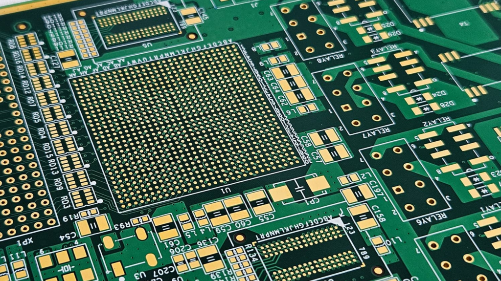
In the fast-evolving landscape of modern electronics, High-Density Interconnect (HDI) PCBs have become indispensable. These sophisticated circuit boards are the backbone of compact, high-performance devices, enabling greater functionality in smaller footprints. From smartphones and wearables to advanced medical equipment and automotive systems, the demand for HDI circuit boards continues to surge. But what precisely allows these intricate boards to achieve such high densities and robust performance? Beyond the visible layers of traces and vias, a critical, often unseen, manufacturing step called the lamination cycle plays a pivotal role. This process is fundamental to how multi-layer PCBs are constructed, and its precision is exponentially more vital in HDI, directly influencing the board’s reliability, electrical performance, and overall lifespan. For users seeking customized HDI PCB solutions or partnering with reliable HDI PCB manufacturers, understanding this core process is key to appreciating the quality and complexity involved.
II. The Lamination Process: A Core Manufacturing Step
At its heart, PCB lamination is the process of bonding multiple layers of conductive (copper) and insulating (prepreg, core) materials together under controlled conditions of heat and pressure. The primary purpose is to transform individual circuit layers into a rigid, monolithic multi-layer structure that can withstand the rigors of assembly and operation.
Key Components Involved in Lamination
The success of the lamination process relies heavily on the quality and characteristics of the materials used:
- Cores: These are typically pre-fabricated, rigid PCB layers that already have etched circuitry on their surfaces. They provide the structural backbone for the subsequent layers.
- Prepreg (Pre-Impregnated Materials): Prepreg is essentially a fiberglass fabric impregnated with a resin (like epoxy, polyimide, or BT-resin) that has been partially cured to a “B-stage” state. During lamination, this resin flows, fills voids, and then fully cures, acting as the dielectric insulator and the adhesive that binds the layers. Different types of prepreg offer varying dielectric constants (Dk), dissipation factors (Df), and resin flow characteristics, which are crucial considerations for high-speed HDI designs.
- Copper Foils: These are typically very thin copper sheets that form the outermost layers of the PCB or are used between prepreg layers to create additional signal planes. For HDI, extremely thin copper foils (e.g., 9 µm or 12 µm) are often preferred to facilitate finer line widths and spaces.
III. The Lamination Cycle Unpacked: Phases and Parameters
The lamination cycle is a meticulously controlled sequence of events, designed to optimize material flow, adhesion, and curing. Any deviation can lead to defects, compromising the final board’s integrity.
A. Pre-Lamination Preparation
Before the actual lamination begins, meticulous preparation is essential:
- Cleaning and Surface Treatment: Inner layers undergo thorough cleaning to remove contaminants and surface treatments (e.g., black or brown oxide) to enhance copper-resin adhesion.
- Accurate Layer Registration and Stacking: Individual layers, along with prepreg and copper foils, are precisely aligned using registration pins or optical alignment systems. This step is critically important for achieving the tight tolerances required for HDI PCBs. The stack is then loaded into a specialized press.
B. The Lamination Cycle Phases
The cycle typically proceeds through distinct phases:
- Heating Phase:
- The stacked materials are heated at a controlled ramp rate. This slow, controlled increase in temperature allows trapped air and volatile gases to escape from the prepreg and prevents thermal shock.
- As the temperature rises, the resin in the prepreg begins to soften and flow. Understanding the glass transition temperature (Tg), where the resin transitions from a rigid to a rubbery state, and the decomposition temperature (Td), beyond which the material degrades, is crucial for selecting appropriate prepreg and defining the temperature profile.
- Pressure Application Phase:
- Once the resin reaches an optimal viscosity, controlled pressure is applied, typically using a hydraulic press. This pressure consolidates the layers, forces out any remaining air, and ensures uniform resin flow, effectively filling all the etched features and microvias.
- The pressure profile often involves an initial low-pressure stage to allow further air escape, followed by a higher consolidation pressure.
- Dwell/Curing Phase (Hold Time):
- The stack is maintained at peak temperature and pressure for a specific duration. This is the critical curing phase where the resin undergoes polymerization and cross-linking, transforming from a viscous liquid to a solid, stable dielectric.
- Ensuring a full resin cure is paramount for achieving the optimal mechanical, thermal, and electrical properties of the HDI PCB. Incomplete curing can lead to delamination, reduced adhesion, and poor electrical performance.
- Cooling Phase:
- The stack is cooled down at a controlled rate while still under pressure. Maintaining pressure during cooling prevents delamination and warpage, as the materials contract.
- Controlled cooling ensures dimensional stability and locks in the final structural integrity of the multi-layer board.
C. Critical Lamination Parameters
The precise control of these parameters is what differentiates a high-quality HDI PCB manufacturer from others:
| Parameter | Description | Importance in HDI |
| Temperature Profile | Ramp rates, peak temperature, dwell time. | Ensures optimal resin flow and complete cure, preventing voids and delamination. |
| Pressure Profile | Initial low pressure, maximum consolidation pressure, hold time under pressure. | Crucial for consolidating layers, expelling air, and filling microvias. |
| Vacuum Application | Evacuating air from the press chamber before and during heating. | Minimizes void formation, particularly vital for fine-pitch HDI with small features. |
IV. HDI-Specific Challenges and Considerations in Lamination
The inherent complexity of HDI PCBs introduces unique challenges to the lamination cycle, demanding specialized expertise from HDI PCB suppliers and HDI PCB factories.
A. Material Flow and Resin Fill for Microvias
- Microvias, which are typically laser-drilled holes with diameters as small as 50 µm, require complete and uniform resin fill during lamination. Insufficient resin flow can lead to trapped air and voids within or around the microvias, significantly compromising their reliability and electrical connectivity.
- HDI PCB manufacturers must select prepregs with appropriate resin content and flow characteristics to ensure optimal fill without excessive “resin starvation” in other areas.
B. Dimensional Stability and Registration Accuracy
- Achieving precise layer-to-layer alignment is paramount for HDI circuit boards due to their fine lines, small pads, and stacked microvias. Even minor misregistrations can render a board unusable.
- Managing the thermal expansion and contraction of different materials during heating and cooling cycles is critical to maintaining accurate registration. Advanced HDI PCB services utilize sophisticated optical alignment systems and compensation techniques.
C. Thermal Expansion Mismatch
- PCBs consist of multiple materials (copper, various resins, fiberglass) each with different Coefficients of Thermal Expansion (CTE). During heating and cooling, these materials expand and contract at different rates.
- This mismatch can induce significant stress within the board, potentially leading to warpage, delamination, or stress fractures in vias and solder joints. Expert HDI PCB manufacturers select compatible materials and meticulously control cooling rates to mitigate these stresses.
D. Managing High Layer Counts and Complex Stack-ups
- Many HDI designs feature high layer counts (e.g., 10, 12, or even 20+ layers) with intricate stack-up configurations. Ensuring uniform temperature and pressure across thick, multi-layered stacks is a significant challenge. Non-uniformity can lead to localized defects.
- Customized HDI PCB designs often push the boundaries of standard lamination capabilities, requiring specialized presses and experienced operators.
E. Void Formation and Delamination Prevention
- Voids (trapped air bubbles) and delamination (separation of layers) are critical defects that can arise from an improperly controlled lamination cycle.
- Common causes include trapped air, excessive volatile gases from incompletely dried materials, insufficient resin flow, or improper pressure application. The use of vacuum presses is a key strategy for HDI PCB manufacturers to minimize void formation.
V. Impact of Lamination Cycle on HDI PCB Performance
The quality of the lamination cycle directly translates into the performance and longevity of the final HDI PCB.
A. Electrical Performance
- Impedance Control: The precise dielectric thickness between copper layers is crucial for maintaining controlled impedance, which is vital for high-speed signal integrity. A well-executed lamination cycle ensures consistent dielectric thickness and uniform resin distribution, which are foundational to achieving target impedance values.
- Reduced Signal Loss: Voids or inconsistent dielectric properties can lead to increased signal loss and crosstalk. A void-free, tightly bonded structure ensures optimal electrical performance.
B. Mechanical Integrity and Reliability
- Enhanced Bond Strength: A properly cured resin forms strong adhesive bonds between layers, significantly enhancing the mechanical integrity of the board and preventing delamination even under thermal or mechanical stress.
- Improved Resistance to Thermal Cycling: HDI boards often operate in environments with varying temperatures. A robust lamination minimizes internal stresses, making the board more resilient to repeated thermal expansion and contraction.
- Reduced Warpage and Twist: Precise control over the cooling phase under pressure is essential to prevent dimensional instability issues like warpage and twist, which can complicate assembly and affect product functionality.
C. Manufacturability and Yield
- Higher Production Yield: A meticulously controlled lamination cycle is directly correlated with higher production yields and reduced scrap rates for HDI PCB manufacturers. This efficiency translates to cost savings and faster delivery for clients seeking HDI PCB services.
- Fewer Defects: Proper lamination minimizes defects such as delamination, voids, and misregistration, reducing the need for costly rework or outright rejection of boards.
VI. Quality Control and Assurance in HDI Lamination
Ensuring the quality of the lamination process involves rigorous control and inspection measures throughout the manufacturing chain, from the HDI PCB factory to the final product.
A. In-Process Monitoring
- Modern lamination presses are equipped with advanced sensors that continuously monitor and record temperature, pressure, and vacuum levels throughout the cycle. This data provides real-time insights and allows for immediate adjustments if parameters deviate from specifications.
- Automated systems ensure consistency and traceability for every lamination batch.
B. Post-Lamination Inspection
After the lamination cycle is complete, various inspection techniques are employed to verify the quality of the bonded structure:
- X-ray Inspection: Non-destructive X-ray imaging is used to check for precise layer registration, identify any trapped air or voids, and verify the integrity of buried features.
- Micro-section Analysis: This involves cutting a small sample of the PCB and polishing it to reveal a cross-section under a microscope. Micro-section analysis provides a detailed view of resin flow, bond line integrity, voiding, and the quality of microvia formation and fill. It’s a critical tool for assessing the internal quality of HDI boards.
- Dimensional Checks: Measurements are taken to verify overall board thickness, warpage, and twist against specifications.
- Adhesion Testing: Destructive tests may be performed on sample coupons to evaluate the bond strength between layers.
VII. Conclusion: The Unseen Pillar of HDI Excellence
The lamination cycle is far more than just a bonding process; it is the fundamental manufacturing step that truly transforms individual layers into a cohesive, high-performance HDI PCB. Its intricate phases and precise parameter control are what enable the miniaturization, signal integrity, and exceptional reliability demanded by today’s advanced electronic devices. For anyone in need of HDI PCB services, whether you are collaborating with HDI PCB suppliers or directly with an HDI PCB factory, a deep understanding and appreciation for the lamination process can help you better evaluate the capabilities of your manufacturing partners.
As electronic devices continue to shrink while demanding ever-increasing functionality, the art and science of the lamination cycle will only become more sophisticated. Collaborating with experienced and technologically advanced HDI PCB manufacturers who prioritize meticulous control over this critical process is paramount to the success of your next high-density interconnect design.

