Unlocking Modern Electronics: What is the Use of a Multilayer PCB?
The primary use of a multilayer PCB (Printed Circuit Board) is to house complex and dense electronic circuits within a compact, miniaturized footprint. By stacking multiple layers of conductive copper and insulating material, engineers can create intricate, high-performance connections for advanced components, significantly improving signal integrity and reducing electromagnetic interference—making them the backbone of virtually all modern high-tech devices.
Table of Contents
- Why Have Multilayer PCBs Become Indispensable?
- What Are the Core Advantages of Using a Multilayer PCB?
- Exploring the Real-World Applications of Multilayer PCBs
- How Is a Multilayer PCB Constructed?
- Are There Any Downsides? A Look at the Disadvantages
- Multilayer vs. Single and Double-Sided PCBs: When to Choose Which?
- The Future is Layered: Concluding Thoughts
Why Have Multilayer PCBs Become Indispensable?
In the early days of electronics, single-sided PCBs were sufficient. Components were large, and circuits were simple. However, the relentless march of technology, driven by consumer demand for smaller, faster, and more powerful devices, created challenges that a single layer of circuitry simply could not solve. Multilayer PCBs emerged not as a luxury, but as a fundamental necessity to overcome the physical limitations of their predecessors.
The Challenge of Miniaturization and Density
The most significant driver for multilayer technology is the push for **miniaturization**. Consider your smartphone, a powerful computer that fits in your pocket. To achieve this, thousands of components must be packed into an incredibly small space. A single or double-sided board would be physically too large to accommodate the required circuitry. A multilayer PCB allows designers to stack vertical “floors” of circuits, creating a high-rise of connectivity that dramatically increases the surface area for routing traces without increasing the board’s length or width. This is the key to achieving high component density—placing more functionality into a smaller physical volume.
The Need for Superior Electrical Performance
As processor speeds increased and data rates soared, signal integrity became a critical concern. On a crowded single-layer board, high-speed signal traces can easily interfere with one another, creating noise, data corruption, and overall poor performance. This phenomenon, known as *crosstalk*, is a major engineering hurdle. Multilayer PCBs solve this by allowing designers to dedicate entire inner layers as **ground planes** and **power planes**. These uninterrupted copper sheets act as a shield, isolating sensitive signal layers from each other, reducing **electromagnetic interference (EMI)**, and providing a stable, low-inductance power distribution network. This structural advantage is essential for high-frequency applications like servers, routers, and advanced computing systems.
What Are the Core Advantages of Using a Multilayer PCB?
The “use” of a multilayer PCB is best understood through its inherent advantages over simpler board types. These benefits directly enable the creation of sophisticated electronics and are the primary reasons engineers choose this technology for demanding projects.
Enhanced Component Density and Reduced Size
As previously mentioned, the ability to layer circuits is the single greatest advantage. This directly translates to smaller and lighter products. By distributing connections across multiple layers, the overall size of the board can be significantly reduced. This not only benefits handheld devices like smartwatches and medical implants but also simplifies the internal layout of larger systems, such as automotive control units and aerospace avionics, where both space and weight are at a premium.
Improved Signal Integrity and EMI Shielding
The dedicated power and ground planes in a multilayer stackup are not just for distributing electricity; they are critical for electrical performance. The ground plane provides a consistent reference for high-speed signals, controlling their impedance and minimizing signal reflections that can corrupt data. It also acts as a shield, absorbing stray electromagnetic radiation from external sources and preventing the board’s own signals from radiating outwards and interfering with other nearby devices. This makes multilayer PCBs essential for meeting strict regulatory compliance standards for EMI emissions.
Greater Design Flexibility and Power Distribution
With more layers to work with, designers have far more freedom in routing traces. They no longer have to find convoluted paths on a single surface to avoid crossing other traces. This simplifies the layout of complex components like Ball Grid Arrays (BGAs), which may have hundreds of connection points. Furthermore, the use of dedicated power planes allows for a much more robust and cleaner power delivery to sensitive integrated circuits, which is crucial for stable operation.
Increased Durability and Reliability
A multilayer PCB is manufactured by laminating several layers together under high temperature and pressure with an epoxy prepreg material. This process creates a single, incredibly rigid, and durable board. This inherent strength makes multilayer boards more resistant to bending and warping than their single-layer counterparts, increasing the overall reliability and longevity of the final product, especially in environments subject to vibration or physical stress.
Exploring the Real-World Applications of Multilayer PCBs
The uses of multilayer PCBs span nearly every sector of the technology industry. Anywhere there is a need for high performance, complex functionality, and a compact form factor, you will find a multilayer board.
From the life-saving precision of medical equipment to the data-crunching power of enterprise servers, these boards are the unsung heroes. The following table illustrates how their specific advantages meet the demands of various industries.
| Industry | Specific Applications | Key Requirements Met by Multilayer PCBs |
|---|---|---|
| Consumer Electronics | Smartphones, Laptops, Tablets, Smartwatches, Gaming Consoles | High Component Density, Miniaturization, Power Efficiency |
| Medical Devices | Pacemakers, MRI Machines, CT Scanners, Infusion Pumps | High Reliability, Compact Size, EMI Shielding, Durability |
| Automotive | Engine Control Units (ECUs), GPS Systems, Infotainment Systems, ADAS | Durability, Resistance to Vibration, High Reliability, Signal Integrity |
| Aerospace & Defense | Avionics, Satellite Systems, Radar Equipment, Guidance Systems | Extreme Durability, Lightweight, High Reliability, Signal Performance |
| Telecommunications | Cell Towers, Routers, Switches, Servers, Base Stations | Superior Signal Integrity, High-Speed Performance, Power Management |
| Industrial & Robotics | Automation Controllers, Robotic Arms, Industrial Sensors | Robustness, Durability, Complex Circuitry, EMI Immunity |
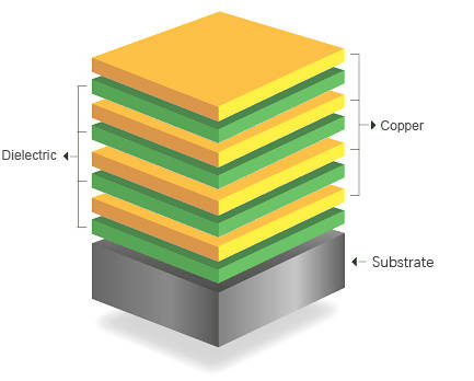
How Is a Multilayer PCB Constructed?
Understanding the construction of a multilayer board further clarifies its use and capabilities. It is not simply a matter of gluing boards together; it is a precise manufacturing process involving lamination and the creation of vertical interconnects.
The Lamination Process: Stacking and Bonding
A multilayer PCB begins as a set of thin, double-sided core layers and sheets of copper foil. The circuit patterns are etched onto the inner core layers first. These etched cores are then alternated with layers of “prepreg”—a fiberglass cloth pre-impregnated with epoxy resin. The entire stack, including the outer copper foil layers, is placed into a lamination press. Under immense pressure and high temperature, the prepreg resin melts, flows, and cures, bonding all the layers into a single, solid board.
Vias: The Vertical Connection Highways
Simply stacking layers isn’t enough; they must be interconnected. This is achieved using **vias**, which are plated-through holes that act as electrical conduits between different layers of the PCB. There are three main types of vias, each offering different design possibilities:
- Through-hole Vias: These are the most common type, drilling from the top layer all the way to the bottom layer, connecting any layers in between.
- Blind Vias: These connect an outer layer to one or more inner layers but do not go all the way through the board. They are essential for freeing up space on layers they don’t connect to.
- Buried Vias: These connect only inner layers and are completely invisible from the outside of the board. Blind and buried vias are key technologies for achieving the highest component densities.
Are There Any Downsides? A Look at the Disadvantages
While incredibly useful, multilayer PCBs are not the solution for every project. Their complexity introduces trade-offs that must be considered during the design and budgeting phases.
Cost and Manufacturing Complexity
The most significant disadvantage is **cost**. The intricate manufacturing process, involving multiple steps of lamination, drilling, and plating, is far more expensive and time-consuming than producing a single or double-sided board. The yield rate can also be lower, as a single defect on an inner layer can render the entire board useless, further driving up the price per unit. This makes them impractical for simple, low-cost electronics.
Design Time and Repair Challenges
Designing a multilayer PCB requires a higher level of expertise and more sophisticated software tools. The designer must manage the complex interplay between layers, considering signal paths, power distribution, and potential interference. Furthermore, once the board is laminated, the inner layers are inaccessible. This makes inspection, debugging, and repair extremely difficult, if not impossible. Any design flaws are costly to correct, often requiring a complete redesign and new manufacturing run.
Multilayer vs. Single and Double-Sided PCBs: When to Choose Which?
The decision to use a multilayer PCB depends entirely on the requirements of the project. A simple circuit for a toy does not need a 12-layer board, just as a high-end server cannot function on a single-sided one.
| Feature | Single-Sided PCB | Double-Sided PCB | Multilayer PCB |
|---|---|---|---|
| Cost | Lowest | Low | Highest |
| Component Density | Very Low | Low to Medium | Very High |
| Design Complexity | Simple | Moderate | High |
| Size & Weight | Largest | Large | Smallest & Lightest |
| Signal Integrity | Poor | Fair | Excellent |
| Typical Use Case | Calculators, Toys, Simple Power Supplies | LED lighting, Industrial Controls, Amplifiers | Computers, Smartphones, Medical Devices, Servers |
The Future is Layered: Concluding Thoughts
In conclusion, the primary use of a multilayer PCB is to serve as the foundation for the complex, high-density, and high-performance electronics that define our modern world. They are the definitive solution to the dual challenges of *miniaturization and electrical performance*. While they come with higher costs and design complexity, their advantages in size, signal integrity, and design flexibility are not just beneficial—they are enabling. Without the ability to stack circuit layers, the powerful, portable, and interconnected devices we rely on every day simply would not exist. As technology continues to advance, the demand for even more layers and more intricate designs will only grow, cementing the multilayer PCB’s role as an indispensable component of future innovation.
multilayer pcb, use of multilayer pcb, what is a multilayer pcb used for, advantages of multilayer pcb, multilayer pcb applications, multilayer printed circuit board, pcb design, signal integrity, component density, EMI shielding

