Multilayer PCBs are indispensable in high-speed electronics, offering a crucial foundation for optimal signal integrity, reduced electromagnetic interference (EMI), and enhanced miniaturization. By strategically stacking multiple conductive layers separated by dielectric materials, these advanced circuit boards address the unique challenges posed by faster clock speeds and higher data rates, enabling the sophisticated performance required in modern computing, telecommunications, and advanced aerospace applications.
In the relentless pursuit of faster processing, higher data throughput, and greater functionality within ever-shrinking footprints, the humble Printed Circuit Board (PCB) has evolved from a simple wiring platform into a highly sophisticated, multi-layered architecture. High-speed electronics, characterized by clock frequencies often exceeding several gigahertz and data transfer rates measured in gigabits per second, present a myriad of design challenges. These include maintaining signal integrity, mitigating electromagnetic interference (EMI), ensuring power delivery network (PDN) stability, and managing thermal dissipation. Multilayer PCBs emerge as the quintessential solution, providing the critical structural and electrical framework necessary to overcome these hurdles and unlock the full potential of advanced electronic systems.
The Inherent Challenges of High-Speed Design
As electronic devices become more complex and operate at higher frequencies, the physical characteristics of the PCB itself become active components influencing system performance. Traditional single- or double-layer PCBs, while cost-effective for simpler applications, are woefully inadequate for high-speed scenarios. The primary challenges they fail to address effectively include:
- Signal Integrity (SI) Issues: At high frequencies, signals are no longer simple voltage levels but complex waveforms susceptible to reflections, crosstalk, and attenuation, leading to data corruption.
- Electromagnetic Interference (EMI): Rapidly switching currents and high-frequency signals generate electromagnetic fields that can interfere with adjacent traces and external systems.
- Power Integrity (PI) Concerns: Stable power delivery becomes critical, as voltage fluctuations can cause logic errors and performance degradation.
- Miniaturization Demands: Packing more functionality into smaller spaces necessitates high-density interconnects (HDIs).
- Thermal Management: Higher component densities and power consumption lead to increased heat generation, requiring effective dissipation strategies.
Multilayer PCBs are engineered specifically to tackle these intricate problems, transforming potential system failures into robust, reliable operation.
Unveiling the Architecture: What is a Multilayer PCB?
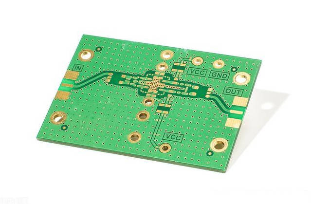
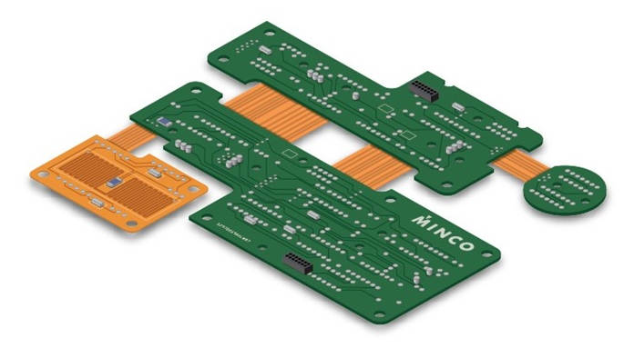
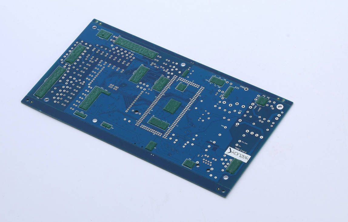
A multilayer PCB is, at its core, a circuit board constructed from three or more conductive copper layers, which are separated and insulated by dielectric (non-conductive) material. These layers are laminated together under high temperature and pressure, forming a single, solid board. The outermost layers are typically used for components and surface routing, while the inner layers are dedicated to signal routing, power planes, and ground planes. The number of layers can range from 4 to 60+, depending on the application’s complexity and performance requirements.
The strategic arrangement of these layers allows designers to create dedicated paths for signals, power, and ground, significantly enhancing control over critical electrical parameters. This layered approach is fundamental to achieving superior performance in high-speed and high-frequency applications.
| Feature | Single/Double Layer PCB | Multilayer PCB |
|---|---|---|
| Signal Integrity | Poor; high crosstalk, reflections. | Excellent; controlled impedance, dedicated ground planes. |
| EMI/EMC | High emission/susceptibility. | Low emission/high immunity; shielding through ground planes. |
| Power Delivery | Limited; voltage drop issues. | Robust; dedicated power/ground planes, low impedance. |
| Component Density | Low. | High; enables miniaturization. |
| Routing Complexity | Simple, limited. | Highly complex, multi-dimensional routing. |
| Cost (per board) | Lower. | Higher (due to complexity). |
| Applications | Simple consumer electronics, LED lighting. | Servers, 5G, medical imaging, aerospace, AI. |
Signal Integrity: The Cornerstone of High-Speed Performance
In high-speed electronics, preserving the integrity of electrical signals is paramount. Any degradation can lead to erroneous data, system instability, or complete functional failure. Multilayer PCBs provide the architectural sophistication required to manage signal behavior effectively.
Controlled Impedance Routing
At high frequencies, PCB traces behave like transmission lines, and their impedance must be carefully matched to that of the components to prevent signal reflections. Reflections occur when a signal encounters a change in impedance, causing part of the signal to bounce back, distorting the original waveform. Multilayer PCBs facilitate controlled impedance routing by allowing designers to precisely control the trace width, trace-to-plane distance, and the dielectric constant of the insulating material. This precision ensures that the signal encounters a consistent impedance throughout its path, minimizing reflections and preserving signal quality.
Dedicated ground and power planes within the stack-up provide a stable reference voltage and a consistent return path for high-frequency currents, which is crucial for maintaining impedance control. Without these planes, the return path would be undefined and erratic, leading to unpredictable impedance variations and severe signal degradation.
Mitigating Crosstalk and Noise
Crosstalk, the unwanted coupling of energy between adjacent traces, is a significant challenge in high-density, high-speed designs. As signals switch rapidly, they generate electromagnetic fields that can induce noise onto nearby traces. Multilayer PCBs mitigate crosstalk through several design strategies:
- Layer Separation: By routing high-speed signals on different layers, or by placing ground planes between signal layers, electromagnetic coupling is physically separated, significantly reducing interference.
- Orthogonal Routing: Routing traces on adjacent layers in orthogonal directions (e.g., horizontal on one layer, vertical on the next) minimizes parallel trace lengths, thus reducing capacitive and inductive coupling.
- Dedicated Ground Planes: Solid ground planes act as effective shields, absorbing radiated EMI and providing low-inductance return paths, which suppresses common-mode noise and reduces the impact of differential-mode noise.
These techniques, made possible by the multilayer structure, are indispensable for preventing data corruption and ensuring reliable communication between high-speed components.
Ensuring Optimal Return Paths
For every signal propagating through a trace, there must be an equivalent return current flowing in the opposite direction, typically through a ground or power plane. In high-speed designs, these return paths must be as direct and unbroken as possible. Discontinuities in the return path (e.g., breaks in a ground plane under a signal trace, or signals changing reference planes through a via without proper stitching) can force the return current to take a longer, higher-inductance path. This creates a “loop antenna” effect, radiating EMI and causing significant signal integrity issues like reflections and excessive propagation delay.
Multilayer PCBs allow for the creation of solid, uninterrupted ground and power planes directly adjacent to signal layers, providing pristine, low-inductance return paths. This direct path minimizes electromagnetic radiation and ensures that signals reach their destination with minimal distortion.
Electromagnetic Compatibility (EMC) and EMI Reduction
High-speed circuits are both sources of and susceptible to electromagnetic interference (EMI). Multilayer PCBs are expertly designed to enhance Electromagnetic Compatibility (EMC) by both reducing the generation of EMI and increasing the immunity of the system to external noise.
Integrated Shielding through Ground Planes
The solid ground and power planes within a multilayer PCB serve as highly effective electromagnetic shields. They contain the electromagnetic fields generated by high-speed signals within the board, preventing them from radiating outwards and interfering with other components or external systems. Conversely, these planes also act as barriers against external EMI, protecting the sensitive internal circuitry. This intrinsic shielding capability is crucial for meeting stringent EMC regulations and ensuring robust system operation in noisy environments.
Minimizing Loop Areas and Radiated Emissions
Any current loop acts as an antenna, radiating electromagnetic energy. In high-speed designs, the signal trace and its associated return path form a current loop. By providing solid ground and power planes directly adjacent to signal layers, multilayer PCBs minimize the area of these current loops. A smaller loop area leads to significantly reduced radiated emissions, improving the overall EMC performance of the system. This direct containment of electromagnetic fields is a fundamental advantage over simpler PCB constructions where return paths can be diffuse and uncontrolled, leading to larger, more effective radiating antennas.
Decoupling Capacitors and Power Plane Effectiveness
Effective decoupling of power rails is essential to prevent noise propagation and maintain stable voltage levels in high-speed circuits. Multilayer PCBs facilitate superior power integrity (PI) through the strategic placement and connection of decoupling capacitors to large, low-inductance power and ground planes. These planes provide a low-impedance path for the high-frequency current required by switching components, acting as charge reservoirs and local energy sources. The close proximity of these planes also creates intrinsic capacitance, known as plane capacitance, which further aids in decoupling at very high frequencies, where discrete capacitors become less effective due to their parasitic inductance. This robust power delivery network (PDN) ensures that high-speed components receive clean, stable power, preventing voltage droop and enhancing overall system reliability.
Miniaturization and High-Density Interconnect (HDI) Capabilities
The demand for smaller, lighter, and more powerful electronic devices drives the need for greater component density and more intricate routing capabilities. Multilayer PCBs are at the forefront of enabling this miniaturization trend through High-Density Interconnect (HDI) technology.
Increased Routing Density
With multiple layers available for routing, designers can accommodate a significantly higher number of traces per unit area compared to single or double-layer boards. This multi-dimensional routing capability allows for complex interconnections between high pin-count components like FPGAs, ASICs, and microprocessors, all within a compact form factor. Without the additional layers, designers would be forced to use much larger board sizes or resort to highly complex and expensive external wiring solutions, which are impractical for most modern devices.
Smaller Form Factors and Reduced Footprints
By routing signals vertically through layers using vias, designers can minimize the overall board size. This capability is critical for consumer electronics, medical devices, and aerospace applications where space is at an absolute premium. A typical 4-layer PCB can achieve routing density far exceeding what a 2-layer board can offer, and advanced multilayer boards with 8, 10, or even 20+ layers are common in devices like smartphones, servers, and high-end graphics cards, enabling unprecedented levels of integration and performance in compact packages.
Via Technologies for HDI
HDI PCBs leverage advanced via technologies to maximize routing density and minimize board size:
- Buried Vias: Connect internal layers without passing through the surface layers, freeing up space on the outer layers for component placement and surface routing.
- Blind Vias: Connect an outer layer to one or more internal layers, but do not pass all the way through the board, again saving space and improving routing flexibility.
- Microvias: Extremely small vias (typically < 150 microns in diameter) created by laser drilling. Microvias enable even finer pitch components and more layers of interconnection within a given space, pushing the boundaries of miniaturization. Stacked microvias allow vertical connections through multiple layers, further enhancing routing density.
These advanced via structures are instrumental in building highly complex, densely packed circuit boards that are essential for today’s cutting-edge electronics.
Enhanced Power Delivery Networks (PDN) and Thermal Management
Beyond signal integrity, multilayer PCBs significantly improve power distribution and offer benefits for thermal management, both critical for reliable high-speed operation.
Robust Power and Ground Planes
Dedicated power and ground planes on internal layers provide low-impedance paths for power delivery and return currents. These large copper planes minimize voltage drop (IR drop) across the board, ensuring that all components receive stable and consistent power, even under high current demands. This is especially vital for sensitive digital circuits where even minor voltage fluctuations can cause errors or instability. The low inductance of these planes also helps filter out high-frequency noise from the power supply, contributing to a cleaner power environment.
Improved Heat Dissipation
While not their primary function, the large copper planes within multilayer PCBs can contribute to improved thermal management. Copper is an excellent thermal conductor, and these planes can help spread heat away from hot spots, distributing it across a larger area of the board. For highly demanding applications, specific layers can be designated as thermal planes or integrated with thermal vias to conduct heat from components to external heatsinks or the board edges for more efficient dissipation. This intrinsic thermal pathway aids in maintaining components within their safe operating temperatures, extending their lifespan and ensuring consistent performance.
Reliability and Manufacturability Advantages
Despite their increased complexity, multilayer PCBs offer significant advantages in terms of reliability and can be efficiently manufactured with modern processes.
Increased Robustness and Durability
The lamination process that binds multiple layers together results in a robust and mechanically stable board. This multi-layered structure is less susceptible to warping and twisting compared to thinner, single-layer boards, especially when subjected to thermal cycling or mechanical stress. This enhanced durability contributes to the long-term reliability of the electronic device, particularly in demanding applications such as automotive, industrial, and aerospace electronics where environmental stresses are common.
Streamlined Manufacturing with Advanced Techniques
While more complex to design, the manufacturing of multilayer PCBs has become highly refined. Automated processes for drilling, plating, and lamination ensure high precision and repeatability. Advances in material science have also led to dielectric materials with tailored electrical properties (e.g., specific Dk and Df values) suitable for high-frequency applications, ensuring predictable signal behavior. Furthermore, the ability to integrate passive components directly into the layers (embedded passives) can further reduce board size and improve performance by shortening interconnections, simplifying assembly, and enhancing manufacturability by reducing the number of surface-mount components.
Applications of Multilayer PCBs in High-Speed Electronics
The essential nature of multilayer PCBs is evident across a broad spectrum of high-speed electronic devices and systems:
- Computing and Servers: High-performance processors, memory modules (DDR4/DDR5), and server motherboards rely heavily on multilayer designs to manage vast amounts of data at blistering speeds, ensuring stable operation and data integrity.
- Telecommunications: 5G base stations, optical transceivers, routers, and high-frequency communication equipment utilize multilayer PCBs for their superior signal integrity and EMI control, vital for reliable wireless and wired data transmission.
- Aerospace and Defense: Avionics, radar systems, satellite communication modules, and guidance systems demand extreme reliability and performance in harsh environments, making multilayer PCBs indispensable.
- Medical Imaging: MRI machines, CT scanners, and ultrasound equipment require precise signal handling for accurate diagnostic imaging, a task perfectly suited for multilayer PCB capabilities.
- Automotive Electronics: Advanced Driver-Assistance Systems (ADAS), infotainment systems, and engine control units (ECUs) leverage multilayer PCBs for their high reliability and ability to process sensor data rapidly.
- Artificial Intelligence and Machine Learning: Specialized AI accelerators and GPU-based systems, processing massive datasets, depend on multilayer PCBs to maintain signal integrity and power delivery for optimal computational throughput.
These diverse applications underscore the critical role multilayer PCBs play in enabling the innovation and functionality of modern high-speed electronics.
The Future Landscape: Evolving PCB Technologies for Even Higher Speeds
As clock speeds continue to rise and data rates push into the terabit range, the demands on PCB technology will only intensify. Future innovations in multilayer PCBs will focus on:
- New Materials: Development of ultra-low loss dielectric materials with improved thermal performance and stability at extremely high frequencies (mmWave, sub-THz).
- Enhanced HDI and Microvia Technology: Further miniaturization of vias and traces, potentially leading to truly 3D interconnects within the board.
- Optical Interconnects: Integration of optical waveguides within the PCB layers to transmit data at light speed, reducing electrical signal loss and latency over longer distances.
- Embedded Components: Greater integration of passive and even active components directly within the PCB substrate, further reducing board size and improving performance.
- Adaptive and Self-Healing PCBs: Boards capable of dynamically adjusting their electrical properties or repairing minor defects.
These advancements will ensure that multilayer PCBs remain the essential backbone of high-speed electronics, continuing to push the boundaries of what is possible in the digital age.
Conclusion: The Unseen Hero of High-Speed Innovation
Multilayer PCBs are far more than just connection platforms; they are sophisticated engineering marvels that form the silent, yet absolutely critical, foundation of high-speed electronics. Their ability to manage complex signal integrity challenges, mitigate EMI, deliver stable power, and facilitate extreme miniaturization makes them indispensable for virtually every advanced electronic device today. As the thirst for faster, smaller, and more powerful technology continues unabated, the evolution of multilayer PCB technology will remain a pivotal enabler, ensuring that the innovations of tomorrow can be reliably brought to life.
Main Keywords: Multilayer PCBs, High-Speed Electronics, Signal Integrity, EMI, Miniaturization, HDI, Power Integrity, PCB Design, Advanced PCBs
Long-Tail Keywords: Why are multilayer PCBs essential for high-speed signal routing?, Benefits of multilayer PCBs in high-frequency applications, How multilayer PCBs reduce EMI in electronic devices, Multilayer PCB advantages for miniaturization, Role of ground planes in high-speed PCB design, Controlled impedance routing in multilayer PCBs, Multilayer PCB vs. single-layer PCB for high-speed, What is HDI PCB technology and why is it used, Multilayer PCB thermal management, Future of PCB technology for high-speed computing, Electromagnetic compatibility in multilayer PCBs.
Synonyms: Stacked PCBs, Multi-layer boards, Advanced circuit boards, High-frequency PCBs, Data integrity, Noise reduction, Compact design, Power delivery network, Stack-up design.
Interrogative Pronouns: What, Why, How, Which.