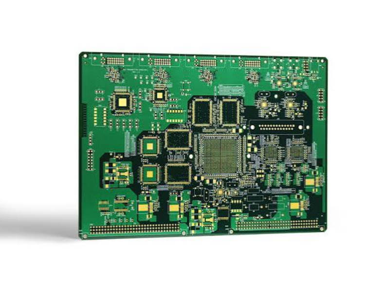
Bookbinder rigid-flex design prevents layer buckling by controlling the length relationship between different layers inside the flexible section. When multilayer flex layers have unequal mechanical paths, compression stress can accumulate and create wrinkles, deformation or long-term reliability issues.
The main reason rigid-flex PCBs develop buckling is layer-length mismatch during bending, not bending itself.
A rigid-flex PCB combines rigid circuit sections with flexible areas, allowing electronic assemblies to fold, move or fit into limited spaces. This structure reduces connectors and improves mechanical integration.
However, designing a reliable rigid-flex PCB requires more than connecting rigid and flexible materials together.
The flexible section contains multiple materials with different mechanical properties:
- copper layers;
- polyimide films;
- adhesive layers;
- coverlay;
- shielding materials;
- stiffeners.
During bending, each layer experiences different levels of tension and compression. If the layers are not mechanically balanced, some layers may become compressed and create buckling.
Bookbinder rigid-flex design is a method used to compensate for these differences by adjusting the effective length of each flexible layer.
Why Rigid-Flex Layer Buckling Happens
Layer buckling usually appears because the flexible section cannot distribute mechanical stress evenly.
Common causes include:
- incorrect layer-length compensation;
- uneven copper distribution;
- excessive flex thickness;
- insufficient bend radius;
- improper layer arrangement;
- uncontrolled lamination movement;
- unsuitable material selection.
A rigid-flex PCB can pass electrical testing while still having hidden mechanical stress inside the flex area.
This is why mechanical design must be considered together with electrical routing.
Understanding Bookbinder Rigid-Flex Design
The term “bookbinder” comes from the behavior of pages inside a book.
When a book bends:
- outer pages travel a longer distance;
- inner pages travel a shorter distance.
The same principle applies to multilayer flexible circuits.
When a rigid-flex PCB bends:
- outer layers experience greater stretching;
- inner layers experience less movement;
- identical layer lengths create mechanical imbalance.
A bookbinder structure intentionally modifies layer lengths so each layer follows a more natural bending path.
The purpose of bookbinder design is not to make every layer equal. It is to make every layer mechanically compatible.
The Relationship Between Layer Length and Flex Reliability
In a multilayer rigid-flex PCB, the neutral axis is the region where bending stress is lowest.
Layers close to the neutral axis experience less strain.
Layers farther away experience higher deformation.
The position of each layer affects:
| Layer Position | Mechanical Effect |
| Near neutral axis | Lowest bending stress |
| Middle flex layers | Moderate strain |
| Outer copper layers | Highest mechanical movement |
| Thick copper planes | Increased stiffness |
A poor layer arrangement can force one layer to compress while another stretches.
Because copper cannot easily compress, excessive compression may result in:
- wrinkles;
- buckling;
- layer movement;
- adhesive stress;
- copper fatigue.
Key Factors That Influence Bookbinder Rigid-Flex Performance
1. Layer-Length Compensation
The most important factor in bookbinder design is controlling the length relationship between flexible layers.
A common mistake is designing all flex layers with identical lengths.
For example:
A four-layer flexible section contains:
- top copper;
- inner dielectric;
- inner copper;
- bottom copper.
Although the layers have the same nominal length in CAD, they do not travel the same distance when bent.
The outer layers require more movement, while inner layers require less.
Layer Compensation Concept
| Layer Location | Design Consideration |
| Outer flex layers | Usually require additional effective length |
| Inner flex layers | Usually require less length |
| Copper-heavy layers | Require additional mechanical review |
| Shielding layers | Must be included in stress analysis |
The exact compensation depends on:
- flex thickness;
- bend radius;
- material properties;
- layer count;
- manufacturing process.
There is no universal compensation value for every rigid-flex PCB.
2. Copper Distribution Balance
Copper is much stiffer than flexible dielectric materials.
Uneven copper distribution can shift the mechanical center of the flex structure.
Typical problems include:
- large ground planes on only one side;
- dense signal routing concentrated on one layer;
- asymmetric shielding;
- different copper density between layers.
Copper Balance Impact
| Copper Condition | Possible Result |
| Balanced copper distribution | More stable bending |
| Heavy copper on one side | Twisting or curvature |
| Large continuous copper area | Reduced flexibility |
| Uneven routing density | Local stress concentration |
Copper balancing should be considered during stackup planning, not after routing is completed.
3. Flex Thickness Control
Adding more layers improves electrical capability but increases mechanical difficulty.
A thicker flex section creates:
- higher bending resistance;
- larger minimum bend radius;
- greater internal stress;
- increased fatigue risk.
Flex Layer Count Consideration
| Flex Structure | Mechanical Behavior |
| Single-layer flex | Maximum flexibility |
| Two-layer flex | Balanced flexibility and routing |
| Multilayer flex | Higher density but increased stiffness |
| Thick multilayer flex | Requires detailed mechanical planning |
A multilayer flex section should only contain the layers required by the electrical design.
4. Bend Radius Design
Bend radius directly affects copper strain.
A smaller bend radius increases:
- copper fatigue;
- dielectric stress;
- adhesive movement;
- risk of cracking.
The correct bend radius depends on:
- copper thickness;
- number of layers;
- flex material;
- whether bending is static or dynamic.
Static vs Dynamic Bending
| Application | Main Design Priority |
| One-time folding | Space optimization |
| Occasional movement | Stress balance |
| Repeated movement | Fatigue resistance |
| Continuous motion | Mechanical validation |
A rigid-flex PCB used in a hinge mechanism requires different design rules compared with a board folded only during assembly.
Bookbinder Design vs Traditional Rigid-Flex Stackup
| Feature | Traditional Rigid-Flex | Bookbinder Rigid-Flex |
| Layer length | Usually identical | Intentionally adjusted |
| Mechanical compensation | Limited | Integrated into design |
| Flex stress control | Depends mainly on materials | Controlled through layer relationship |
| Design complexity | Lower | Higher |
| Manufacturing planning | Standard rigid-flex process | Requires advanced stackup control |
| Best application | Simple flex sections | Multilayer bending applications |
Bookbinder design is not necessary for every rigid-flex PCB.
It becomes valuable when:
- multiple flex layers are stacked;
- the bending radius is limited;
- the flexible section is thick;
- reliability requirements are high.
How to Design a Reliable Bookbinder Rigid-Flex PCB
1. Define Mechanical Requirements Before Routing
Before starting PCB layout, confirm:
- bending direction;
- installation space;
- minimum bend radius;
- expected movement cycles;
- static or dynamic application.
The mechanical requirements should guide the electrical design.
2. Optimize Layer Arrangement
The layer order strongly affects stress distribution.
Engineers should review:
- copper layer position;
- plane placement;
- coverlay thickness;
- adhesive thickness;
- stiffener location.
Sensitive signal layers should avoid unnecessary mechanical stress zones.
3. Control Copper Density
Recommended practices include:
- balancing copper distribution;
- avoiding unnecessary large copper areas;
- reviewing shielding structures;
- maintaining similar copper density between layers.
This reduces uneven deformation during bending.
4. Design the Rigid-Flex Transition Carefully
The transition between rigid and flexible sections is often the highest stress area.
Potential problems:
- abrupt thickness changes;
- copper extending too close to the bend area;
- insufficient support;
- improper stiffener placement.
A smooth transition reduces stress concentration.
Common Bookbinder Rigid-Flex Design Mistakes
Mistake 1: Treating Flex Areas Like Thin Rigid Boards
A flexible section is a mechanical component.
Electrical connection alone does not guarantee reliability.
Mistake 2: Ignoring Layer Sequence
Two rigid-flex designs with identical layer counts can behave differently because layer position changes mechanical stress.
Mistake 3: Adding Copper After Mechanical Design
Late changes such as:
- adding ground planes;
- increasing power copper;
- modifying shielding;
can destroy the original mechanical balance.
Mistake 4: Using Excessive Flex Layers
More layers increase routing capability but reduce flexibility.
Mistake 5: Ignoring Manufacturing Capability
Bookbinder structures require accurate control of:
- layer registration;
- lamination pressure;
- adhesive flow;
- material thickness.
A design that works theoretically may fail during manufacturing without suitable process capability.
Manufacturing Considerations for Bookbinder Rigid-Flex PCB
A reliable rigid-flex PCB requires cooperation between designers and manufacturers.
Important manufacturing factors include:
Stackup Control
Confirm:
- layer sequence;
- dielectric thickness;
- copper thickness;
- coverlay structure;
- adhesive thickness.
Lamination Control
During pressing:
- materials expand differently;
- adhesive flows;
- copper patterns affect pressure distribution.
Poor control may create:
- wrinkles;
- layer movement;
- thickness variation.
Registration Accuracy
Multilayer rigid-flex structures require accurate alignment because small layer movement can affect:
- impedance;
- bending behavior;
- mechanical balance.
Prototype Validation
Testing should evaluate:
- bending performance;
- visual deformation;
- electrical continuity;
- mechanical durability.
How to Choose a Rigid-Flex PCB Manufacturer
A suitable manufacturer should understand both electrical and mechanical requirements.
Important evaluation points include:
| Capability | Why It Matters |
| Multilayer rigid-flex experience | Understands complex flex structures |
| Stackup engineering | Helps optimize layer arrangement |
| Lamination control | Reduces deformation risk |
| Flex material handling | Prevents mechanical damage |
| DFM review ability | Identifies problems before production |
Before production, provide:
- layer stackup;
- flex dimensions;
- bend requirements;
- copper distribution;
- application environment;
- reliability requirements.
A manufacturer experienced in Rigid-Flex PCB manufacturing can help evaluate layer balance, stackup design and fabrication risks before mass production.
FAQ
What is bookbinder rigid flex design?
Bookbinder rigid-flex design adjusts the length relationship between flexible layers to reduce compression stress and prevent buckling during bending.
Why does a rigid-flex PCB buckle?
Rigid-flex buckling usually happens because different layers have different mechanical lengths, copper distribution imbalance, excessive thickness or insufficient bend radius.
How does layer-length compensation prevent flex PCB buckling?
Layer-length compensation allows different layers to follow their natural bending paths, reducing compression stress inside the flexible section.
Is bookbinder design required for every rigid-flex PCB?
No. Simple rigid-flex designs may not require it. Bookbinder structures are mainly used for multilayer flex sections with complex bending requirements.
Does copper thickness affect rigid-flex reliability?
Yes. Thicker copper increases stiffness and can increase bending stress, especially in multilayer flexible sections.
Can rigid-flex PCB buckling happen after fabrication?
Yes. Some problems appear during assembly, bending or thermal cycling because mechanical stress accumulates after manufacturing.
What information should be provided for rigid-flex PCB manufacturing?
Provide stackup information, flex dimensions, bend requirements, layer count, copper thickness and application conditions.
How can designers improve rigid-flex bending reliability?
Designers should balance copper, optimize layer sequence, control bend radius and work with manufacturers during stackup planning.
Conclusion
Bookbinder rigid-flex design is a mechanical optimization method that helps multilayer flexible circuits survive bending without layer buckling.
The key is not simply adding more flexible layers. The entire structure must be balanced:
- layer lengths;
- copper distribution;
- bend radius;
- material thickness;
- stackup sequence.
A reliable rigid-flex PCB starts with mechanical planning before electrical routing begins.
When a flexible section requires complex bending or multilayer construction, early stackup review can prevent costly redesigns.
For rigid-flex projects requiring controlled layer structures and manufacturing support, review the design requirements with Mars-PCB through the Rigid-Flex PCB manufacturing service.