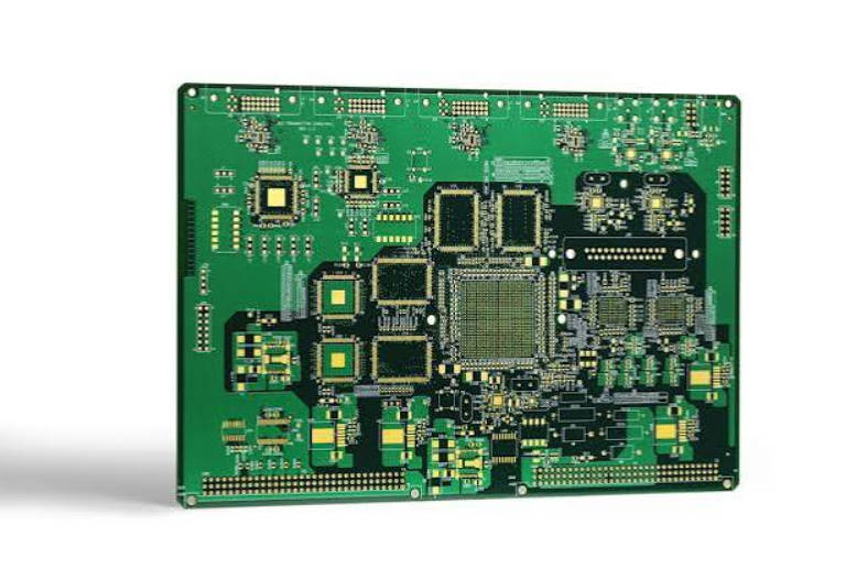
Staggered microvias are generally the lower-risk option when the intermediate layer has enough routing space for an offset connection. Stacked microvias are more appropriate when fine-pitch BGAs, restricted board area or Any-Layer routing require multiple microvias to occupy the same X-Y location.
The central trade-off is simple: staggered microvias consume more lateral routing space, while stacked microvias consume more manufacturing and reliability margin.
A stacked microvia is drilled directly above a filled microvia on the previous layer. A staggered structure offsets the next microvia and connects the two vias with a short trace or landing feature on the intermediate layer.
Both structures can be manufactured reliably. The difference is that stacked designs depend more heavily on copper filling, surface planarity, registration and the integrity of the interface between one microvia and the next.
Industry investigations have identified weak microvia-to-target-pad interfaces as a potential source of latent failure, particularly in compound and stacked structures. Some failures have appeared only after assembly reflow or thermal testing, even though the boards previously passed conventional bare-board inspection.
For this reason, the decision should not be reduced to a simple drawing preference. It must consider where the interconnect could fail, how much routing area is available and how the completed board will be tested.
Begin with the Cross-Section, Not the Via Symbol
In a PCB layout tool, stacked and staggered microvias may appear as small pad shapes connected across layer pairs. Their physical cross-sections are significantly different.
Stacked Microvia Structure
A typical two-level stacked structure may contain:
- A laser-drilled microvia from Layer 3 to Layer 2;
- Electrolytic copper filling inside that microvia;
- Planarization or controlled copper capping;
- A second buildup layer;
- Another laser-drilled microvia from Layer 2 to Layer 1, positioned directly above the first.
The lower microvia must provide a stable, sufficiently flat target for the upper laser drill and plating process.
Staggered Microvia Structure
A staggered structure places the Layer 1-to-Layer 2 microvia beside the Layer 2-to-Layer 3 microvia. A copper connection on Layer 2 links them.
The upper microvia therefore terminates on an ordinary target land rather than directly on top of a previously filled microvia.
Structural Comparison
| Design Feature | Stacked Microvias | Staggered Microvias |
| X-Y position | Vertically aligned | Laterally offset |
| Intermediate-layer routing area | Minimal | Requires connecting land or trace |
| Copper fill requirement | Normally essential for the lower via in the stack | May be avoided in some structures, unless via-in-pad or planarity requires fill |
| Surface planarity | Critical | Less dependent on the previous via surface |
| Registration demand | Very high | High, but errors do not accumulate on one vertical axis in the same way |
| Number of plated interfaces | Concentrated in one vertical structure | Distributed across separate vias and a trace |
| Routing density | Higher | Lower |
| Typical cost direction | Higher | Lower when additional fill and planarization are avoided |
| Reliability qualification | More demanding as stack height increases | Generally more straightforward |
| Main use case | Tight BGA escape, ELIC and restricted board area | Reliability-focused HDI with available lateral space |
A stacked microvia saves space by placing several manufacturing interfaces in the same vertical path.
Failure Path 1: Separation at the Target-Pad Interface
The most important stacked-microvia failure does not necessarily occur through the center of the copper fill. It may occur at the interface where the microvia terminates on its target pad.
During lamination, reflow and thermal cycling, copper and the surrounding dielectric expand at different rates. This creates mechanical stress around the microvia base, capture pad and target pad.
In a stacked structure, the rotation and deformation of one pad can affect the next via directly above it. Published reliability work has observed a greater tendency toward corner cracking in certain copper-filled stacked configurations and has identified more potential failure modes as microvias are stacked on one another or on a buried via.
A weak interface may be caused or aggravated by:
- inadequate target-pad cleaning;
- weak electroless-copper deposition;
- contamination remaining after laser drilling;
- poor adhesion between the target pad and copper fill;
- excessive microvia aspect ratio;
- high dielectric Z-axis expansion;
- repeated lamination and reflow exposure;
- plating chemistry variation.
The failure may behave intermittently. A crack can open at elevated temperature and partially close after the board cools, making room-temperature electrical testing less effective at detecting it.
A microvia that passes continuity testing before assembly is not automatically proven reliable after lead-free reflow.
Failure Path 2: Voids and Uneven Copper Filling
Stacked microvias require the lower via to support the next buildup level. This normally means filling the lower microvia with electrolytic copper rather than leaving a conformal plated depression.
Copper filling must create:
- complete internal fill;
- minimal voiding;
- controlled surface dimple;
- adequate cap copper;
- uniform plating thickness;
- a suitable target for the next laser drill.
Large voids create localized stress concentrations inside the deposited copper. One published analysis found that significant voiding could dramatically reduce predicted microvia fatigue life, while interface delamination remained another major failure mechanism. The exact impact depends on void size, location and geometry.
Common Copper-Fill Defects
| Defect | Why It Matters |
| Internal void | Concentrates thermomechanical stress and reduces load-bearing copper |
| Deep surface dimple | Creates an uneven target for the next stacked via |
| Copper bump | Interferes with dielectric thickness and local planarity |
| Thin copper at the via base | Weakens the target-pad connection |
| Incomplete fill | Prevents reliable stacking and may trap process residues |
| Excessive cap thickness | Alters local layer thickness and fine-feature imaging |
| Nonuniform fill across the panel | Produces variable reliability between board locations |
Copper filling is now an established HDI production process, but it remains a controlled electrochemical operation rather than a simple extension of through-hole plating.
Why Staggering Can Simplify the Structure
In a staggered design, the next microvia does not need to be drilled directly onto the previous via. The lower microvia may therefore avoid some of the structural support requirements associated specifically with stacking.
This does not mean staggered microvias never require filling. Copper or nonconductive fill may still be necessary when:
- the microvia is inside a component pad;
- the surface must be planar for soldering;
- assembly voiding must be controlled;
- the fabrication standard requires filled structures;
- another process step depends on a flat surface.
The cost advantage must therefore be calculated from the actual via-in-pad and filling requirements, not from the word “staggered” alone.
Failure Path 3: Excessive Microvia Aspect Ratio
A microvia is a blind structure with a controlled depth-to-diameter relationship. IPC design documentation uses a maximum 1:1 aspect-ratio boundary and a maximum depth of 0.25 mm for the microvia definition. The applicable production limit may be more conservative.
A 1:1 limit should not be interpreted as the preferred production target.
An IPC-published study comparing several materials and microvia geometries found substantially stronger thermal-test performance for certain 0.5:1 structures than for 1:1 structures made with the same material. The study also showed that dielectric material and Z-axis expansion had a strong influence on reliability.
For example:
- A 75 µm finished laser diameter through 75 µm of dielectric produces a 1:1 aspect ratio.
- The same diameter through 50 µm of dielectric produces approximately 0.67:1.
- Increasing the finished diameter or reducing the dielectric thickness generally widens the plating and filling process window.
These examples are geometric illustrations, not universal manufacturing limits.
Design Variables That Control Aspect Ratio
- Finished laser-via diameter;
- Laser-drilled opening before metallization;
- Buildup dielectric thickness;
- Copper foil thickness;
- Target-pad depth;
- Final copper-fill geometry;
- Fabricator-specific laser and plating capability.
For stacked structures, every microvia level must meet its own practical aspect-ratio requirement. A three-level stack is not one 3:1 microvia; it is a sequence of separate microvias, each of which must be drilled, cleaned, plated and filled correctly.
Failure Path 4: Accumulated Registration Error
Stacked microvias must align across several independently processed buildup layers.
Each level introduces variation from:
- artwork scaling;
- dielectric movement;
- sequential lamination;
- laser-drill registration;
- copper plating;
- imaging alignment;
- panel distortion.
A small positional shift at one buildup level can reduce the effective annular ring or move the upper laser via toward the edge of its lower target.
Staggered microvias also require accurate registration, but the designer can often provide a larger intermediate pad or short connecting trace. The next microvia is not forced to land on the center of the previous filled via.
Registration Risk by Structure
| Structure | Registration Sensitivity |
| Single microvia | One laser-to-target alignment |
| Two staggered microvias | Two alignments plus an intermediate copper connection |
| Two stacked microvias | Two alignments concentrated on the same vertical target |
| Microvia stacked on buried via | Laser alignment plus buried-via and buildup registration |
| Multi-level stacked structure | Repeated alignment across several sequential processes |
The practical maximum stack height is therefore supplier- and process-specific. There is no responsible universal answer such as “four stacked microvias are always safe.”
Published studies have successfully tested some multi-level stacked structures, while other work has emphasized that the number of possible failure modes and manufacturing difficulty increases as stacks become taller.
Failure Path 5: Repeated Lamination and Thermal Exposure
A two-level HDI buildup requires multiple fabrication stages. Higher-order HDI and ELIC structures require additional sequential cycles.
A simplified sequence may include:
- Fabricating the inner core;
- Laminating a buildup dielectric;
- Laser drilling;
- Desmear or residue removal;
- Metallization;
- Copper filling;
- Planarization and imaging;
- Adding the next dielectric;
- Repeating the process.
Every cycle exposes existing materials and copper structures to additional temperature and pressure.
This can affect:
- dielectric expansion;
- resin condition;
- copper grain structure;
- interface stress;
- registration;
- board flatness;
- buried-via reliability.
A stacked structure concentrates the consequences of these cycles into a vertically connected interconnect. A staggered structure distributes the path across separate via locations, although it remains subject to the same general sequential-lamination environment.
The Space Audit: What Staggered Microvias Cost in the Layout
Staggered microvias usually improve the structural risk profile by purchasing reliability with routing area.
The intermediate layer requires space for:
- two capture or target lands;
- the offset between via centers;
- a connecting trace or copper neck;
- clearance to adjacent signals;
- plane anti-pads where applicable.
This can become difficult under:
- 0.4 mm or smaller BGAs;
- high-pin-count processors;
- memory packages;
- compact camera modules;
- mobile devices;
- narrow board outlines;
- tightly packed differential pairs.
Example of the Routing Conflict
Suppose a signal must travel from Layer 1 to Layer 3.
With stacked microvias, the Layer 1-to-Layer 2 and Layer 2-to-Layer 3 vias share the same X-Y coordinate. Very little routing area is consumed on Layer 2.
With staggered microvias, Layer 2 must contain a horizontal connection between the two via centers. That connection may block another escape channel or violate clearance beneath a dense BGA.
Staggering is preferable only when the intermediate layer can afford the offset without creating a different manufacturability problem.
The Cost Audit: What Stacked Microvias Add
The price difference cannot be calculated accurately from the via count alone.
Stacked microvias may add cost through:
- mandatory copper filling;
- tighter dimple and planarity requirements;
- additional plating control;
- more demanding laser registration;
- inspection of every stacked interface;
- sequential buildup cycles;
- lower process yield;
- reliability coupons and thermal testing;
- a smaller qualified supplier base.
Staggered microvias may reduce some of these requirements, but they can also increase:
- board area;
- layer count;
- routing congestion;
- trace length;
- design time.
Relative Cost Drivers
| Cost Driver | Stacked | Staggered |
| Laser drilling | High | High |
| Sequential lamination | High | High |
| Copper filling | Usually higher | Structure-dependent |
| Planarization | Critical | Less critical unless via-in-pad |
| Registration control | Very high | High |
| Intermediate routing space | Low | High |
| Potential board-size reduction | High | Moderate |
| Reliability qualification | Higher as stack levels increase | Generally lower |
| Layout complexity | Lower in tight vertical transitions | Higher where offsets compete for routing |
| Fabrication yield sensitivity | Higher | Lower in many comparable structures |
Stacked microvias can still reduce total product cost when they allow a smaller PCB, fewer layers or the use of a required fine-pitch package. The correct comparison is therefore total system cost, not only PCB unit price.
When Stacked Microvias Are Justified
Use stacked microvias when the design genuinely needs vertical density.
Typical reasons include:
- The BGA escape has no room for an offset;
- Several buildup layers must be reached from the same pad location;
- Any-Layer or ELIC routing is required;
- A staggered connection would block another critical channel;
- The product outline cannot be enlarged;
- Reducing layer count creates enough value to offset the process cost;
- The selected supplier has a qualified stacked-microvia process.
Stacked microvias are particularly common in compact electronics, dense computing modules, mobile products and advanced interconnect structures.
A project using multiple stacked levels should receive a supplier-specific HDI microvia design review before the pad stack and layer pairs are frozen.
When Staggered Microvias Are the Better Choice
Prefer staggered microvias when:
- the intermediate layer has sufficient routing area;
- long vertical stacks are not necessary;
- thermal reliability is a major program priority;
- supplier capability for multi-level stacking is uncertain;
- board size is less important than process margin;
- the product will experience demanding reflow or thermal cycling;
- the cost of copper filling and qualification is difficult to justify.
Staggered structures are especially useful in industrial, automotive, medical and aerospace designs where a modest increase in routing area may be acceptable in exchange for a simpler interconnect path.
Design Rules to Confirm Before Layout Release
Do not copy generic microvia dimensions from another project.
Confirm the following with the selected HDI and ELIC PCB manufacturer:
Microvia Geometry
- Finished laser-via diameter;
- Buildup dielectric thickness;
- Permitted aspect ratio;
- Capture-pad diameter;
- Target-pad diameter;
- Minimum annular ring;
- Laser-drill positional tolerance.
Stacked Structure
- Maximum qualified number of stacked levels;
- Copper-fill method;
- Maximum permitted fill void;
- Dimple or bump tolerance;
- Cap-plating thickness;
- Planarization method;
- Whether stacking over a buried via is permitted;
- Buried-via fill and cap requirements.
Staggered Structure
- Minimum center-to-center offset;
- Intermediate connecting-trace width;
- Minimum copper neck;
- Clearance to adjacent pads and anti-pads;
- Whether the lower microvia requires filling;
- Plane-clearance requirements.
Material and Lamination
- Buildup dielectric;
- Z-axis CTE;
- Lamination temperature;
- Number of sequential cycles;
- Finished dielectric tolerance;
- Registration compensation.
IPC-2226A establishes design considerations for HDI printed boards, including microvia formation, metallization and staggered structures, but final dimensions still need to reflect the selected fabricator’s qualified process.
Do Not Use Microsections as the Only Reliability Evidence
A polished cross-section can reveal:
- gross voids;
- misregistration;
- copper thickness;
- obvious cracks;
- target-pad condition.
It examines only a limited physical location and may not reproduce the temperature-dependent behavior of a latent interface defect.
Industry warnings have noted that thermally stressed microsections and light-microscope inspection alone may fail to detect weak microvia interfaces. Performance-based via-chain testing with resistance monitoring during reflow simulation or thermal cycling can provide stronger evidence.
A More Complete Verification Plan
| Verification Method | What It Evaluates |
| Microsection | Geometry, copper thickness, voids and registration |
| X-ray or suitable nondestructive inspection | Gross fill and alignment abnormalities |
| Reflow simulation | Assembly-temperature survival |
| Thermal cycling | Fatigue under repeated temperature change |
| Via-chain resistance monitoring | Intermittent or temperature-dependent interface opening |
| Lot-specific coupons | Actual production panel process |
| Failure analysis | Exact crack location and mechanism |
The test coupon should reproduce:
- the same microvia diameter;
- the same buildup dielectric;
- the same stack height;
- the same copper-fill process;
- the same target-pad construction;
- the same lamination sequence.
A simple single-level coupon does not fully qualify a product containing a four-level stacked structure.
Questions to Include in the RFQ
Ask the PCB manufacturer:
- How many stacked microvia levels are qualified in regular production?
- Is the proposed stack based on existing production data or only prototype feasibility?
- What aspect ratio is preferred rather than merely possible?
- How are fill voids, dimples and cap thickness controlled?
- Can microvias be staggered in selected locations to reduce stack height?
- Is stacking over a mechanically drilled buried via permitted?
- How is the buried via filled and planarized?
- Which buildup material is proposed?
- How many sequential lamination cycles are required?
- Which coupons will be placed on the production panel?
- Is resistance monitored during thermal testing?
- What changes require customer approval before production?
Mars-PCB lists stacked and staggered microvia planning, sequential buildup structures and Any-Layer ELIC among the design and manufacturing considerations for its HDI service. The exact structure still needs a project-specific DFM assessment.
Common Design Mistakes
Stacking Every Microvia by Default
Vertical alignment may make the layout cleaner, but it introduces fill and interface requirements even where lateral space is available.
Staggering Without Checking Escape Congestion
The offset may consume the only routing channel beneath a fine-pitch BGA.
Using the 1:1 Aspect Ratio as a Design Target
A maximum definition is not the same as a robust production target. Lower ratios can provide a wider plating and reliability margin.
Specifying Copper Fill Without a Dimple Limit
A filled microvia can still provide a poor target for the next level if its surface is deeply concave or excessively raised.
Stacking on an Unfilled Buried Via
The buried structure must provide a stable, planar foundation for the microvia above it.
Assuming More Stacked Levels Only Affect Cost
Every level adds an interface, alignment operation and thermal-mechanical dependency.
Testing a Different Structure from the Product
A single-level microvia coupon does not qualify a multi-level stack.
Changing the Buildup Dielectric After Routing
A change in dielectric thickness alters aspect ratio, pad size, impedance and registration assumptions.
Selection Matrix
| Project Condition | Recommended Starting Point |
| Intermediate layer has sufficient offset space | Staggered |
| Tight 0.4 mm or smaller BGA escape | Evaluate stacked |
| Long product life with severe thermal cycling | Prefer staggered where routing permits |
| Any-Layer ELIC architecture | Stacked is often required |
| Cost-sensitive HDI with moderate density | Staggered or single-level microvias |
| Board outline cannot increase | Stacked may justify the added process |
| Unqualified supplier process | Avoid tall stacks |
| Via-in-pad beneath fine-pitch package | Copper-filled structure required; compare stacked and staggered options |
| Thick board with stacked microvia over buried via | Requires detailed reliability review |
| High-volume product with mature ELIC supplier | Stacked may be commercially practical |
FAQ
Are stacked microvias less reliable than staggered microvias?
Stacked microvias generally have more interface and plating dependencies. They can be reliable when the geometry and process are qualified, but staggered structures often provide a wider reliability margin when routing space is available.
Why must stacked microvias be copper filled?
The lower microvia must provide a solid, planar target for the next laser-drilled via. Copper filling supports the upper structure and creates the electrical connection between stacked levels.
Do staggered microvias need copper filling?
Not always. Filling may still be required for via-in-pad, surface planarity, assembly control or a specific fabrication standard. A staggered position alone does not determine the fill requirement.
What is a safe microvia aspect ratio?
IPC design references define a microvia using a maximum 1:1 aspect ratio, but many production processes target a more conservative ratio. The final limit must be confirmed with the selected manufacturer.
How many microvias can be stacked?
There is no universal safe number. The answer depends on material, via geometry, copper filling, registration, lamination sequence and the manufacturer’s qualified reliability data.
Are two stacked microvias reliable?
A two-level stack is widely manufacturable, but reliability still depends on target-pad preparation, fill quality, aspect ratio and thermal qualification. It should not be approved from stack height alone.
Are staggered microvias cheaper than stacked microvias?
They are often less expensive when they avoid copper filling, tight planarization and highly concentrated registration. The final cost may increase if staggering requires a larger board or more routing layers.
Can stacked microvias be placed over buried vias?
Yes, but the buried via normally requires suitable filling and capping to create a stable foundation. This compound structure needs tighter process and reliability control.
What causes stacked microvia failure?
Common causes include weak target-pad interfaces, copper-fill voids, high aspect ratio, poor hole cleaning, plating variation, accumulated misregistration and thermomechanical stress.
How should microvia reliability be tested?
Use representative via-chain coupons exposed to reflow simulation or thermal cycling while monitoring electrical resistance. Microsections should support—not replace—performance-based testing.
Conclusion
The stacked vs staggered microvia decision is a choice between two different resources.
Staggered microvias consume intermediate-layer area but reduce dependence on a vertical chain of filled and plated interfaces. Stacked microvias preserve routing space and enable dense layer access but require stronger copper-fill, registration and reliability controls.
Use staggered microvias wherever the offset can be routed cleanly; use stacked microvias where vertical density creates a measurable layout or product advantage.
Before releasing the design, define the microvia diameter, dielectric thickness, fill requirement, permitted stack height, dimple tolerance and thermal qualification method.
For a feasibility review, submit the stackup, BGA pitch, via map and assembly profile through the Mars-PCB website so that routing density and microvia reliability can be evaluated together.